


SA-1110 Developer’s Manual 133
Memory and PC-Card Control Module
15..4 DRI 11..0
DRAM refresh interval, all banks.
Number of memory clock cycles (divided by 32) between CAS before RAS (CBR) refresh
cycles. One row is refreshed in each DRAM bank during each CBR refresh cycle. This
interval is applicable to asynchronous and/or synchronous DRAM in all four banks.
The value that must be loaded into this register is calculated as follows:
DRI = Number of cycles /32 = ((Refresh time - longest burst access time) / rows) x Memory
clock frequency /32. The longest burst access time to subtract must consider full burst
accesses to DRAM and SMROM. It must also consider 32-bit word accesses (either
nonburst or within a burst) to ROM, Flash, SRAM, or variable latency I/O. The longest
access time for variable latency I/O includes the maximum number of wait cycles caused
by deassertion of the RDY pin. Thus, indefinitely long deassertions of the RDY pin will
prevent refresh and may corrupt the DRAM contents.
ROM, Flash, SRAM, or variable latency I/O transfers may be interrupted to service a
DRAM refresh cycle after each 32-bit word. If there is a read on a 16-bit bus, a refresh
cycle may be inserted after 2 read cycles. If there is a read to a 32-bit bus, the refresh waits
one read cycle to be serviced. The DRAM interface inserts CBR refresh cycles between
bursts of up to 8 words. Since the address pins are ignored by DRAM during CBR refresh
cycles, PC-Card transactions may be ongoing during a refresh cycle and will not be
interrupted.
16 E0PIN
SMROM clock enable pin 0 (SDCKE 0) level control/status.
Control/status bit for the SDCKE 0 pin and it is automatically cleared upon entering sleep
mode. It is set upon hardware or sleep reset if static memory bank 0 (boot space) is
configured for SMROM (SMROM_EN = 1); otherwise, it is cleared upon hardware or sleep
reset.
E0PIN can be cleared by program to cause a power-down command (if K0RUN=1).
However, this capability should be used with extreme caution because the resulting state
prohibits automatic transitions for mode register set and read commands. E0PIN can be
set by program to cause a power-down-exit command (if K0RUN=1). See Section 10.6.11.
17 K0RUN
SMROM clock pin 0 (SDCLK 0) run control/status.
Control/status bit for operation (run or not) of SDCLK 0 and it is automatically cleared upon
entering sleep mode. It is set upon hardware or sleep reset if static memory bank 0 (boot
space) is configured for SMROM (SMROM_EN = 1); otherwise, it is cleared upon hardware
or sleep reset.
K0RUN can be cleared by program, but this capability should be used with extreme caution
because the resulting state prohibits automatic transitions for any commands. See
Section 10.6.11.
18 K0DB2
SMROM clock pin 0 (SDCLK 0) divide by 2 control/status.
Control/status bit for clock divisor of SDCLK 0. When set, SDCLK 0 runs at one-half the
memory clock frequency. When clear, SDCLK 0 runs at the memory clock frequency. This
bit is automatically set upon hardware or sleep reset.
19 — Reserved.
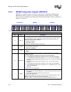
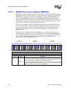
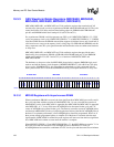
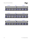
0h A000 001C MDREFR Read/Write
31 30 29 28 27 26 25 24 23 22 21 20 19 18 17 16 15 14 13 12 11 10 9 8 7 6 5 4 3 2 1 0
SLFRSH
Reserved
KAPD
EAPD
Reserved
K2DB2
K2RUN
Reserved
Reserved
K1DB2
K1RUN
E1PIN
Reserved
K0DB2
K0RUN
E0PIN
DRI11
DRI10
DRI9
DRI8
DRI7
DRI6
DRI5
DRI4
DRI3
DRI2
DRI1
DRI0
TRASR3
TRASR2
TRASR1
TRASR0
Reset 1 ? 0 0 ? 1 0 ? ? 1 0 0 ? 1 * * ? ? ? ? ? ? ? ? ? ? ? ? ? ? ? ?
* Upon hardware or sleep reset, K0RUN and E0PIN are set to the value of the SMROM_EN pin.
(Sheet 2 of 4)
Bits Name Description