


252 SA-1110 Developer’s Manual
Peripheral Control Module
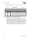
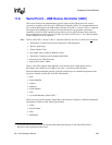
11.7.12 LCD Controller Register Locations
Table 11-10 shows the registers associated with the LCD controller and the physical addresses used
to access them.
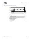
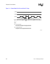
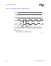
Figures 11-9 to Figure 11-13 describe the LCD controller timing parameters.
6 IOU
Input FIFO overrun upper panel status.
0 - Input FIFO for the upper or whole panel display has not overrun.
1 - DMA attempted to place data into the input FIFO for the upper or whole panel after it
has been filled.
7IUU
Input FIFO underrun upper panel status.
0 – Input FIFO for the upper or whole panel display has not underrun.
1 – DMA not supplying data to input FIFO for the upper or whole panel at a sufficient rate.
FIFO has completely emptied; pixel unpacking logic has attempted to take added data from
the FIFO.
8 OOL
Output FIFO overrun lower panel status.
0 – Output FIFO for the lower panel display has not overrun.
1 – Dither logic attempted to place data into the output FIFO for the lower panel after it had
been filled.
9OUL
Output FIFO underrun lower panel status.
0 – Output FIFO for the lower panel display has not underrun.
1 – LCD dither logic not supplying data to output FIFO for the lower panel at a sufficient
rate. FIFO has completely emptied and data pin driver logic has attempted to take added
data from the FIFO.
10 OOU
Output FIFO overrun upper panel status.
0 – Output FIFO for the upper or whole panel display has not overrun.
1 – Dither logic attempted to place data into the output FIFO for the upper or whole panel
after it had been filled.
11 OUU
Output FIFO underrun upper panel status.
0 – Output FIFO for the upper or whole panel display has not underrun.
1 – LCD dither logic not supplying data to output FIFO for the upper or whole panel at a
sufficient rate. FIFO has completely emptied and data pin driver logic has attempted to take
added data from the FIFO.
31..12 — Reserved.
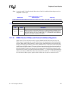
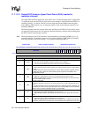
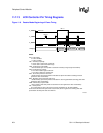
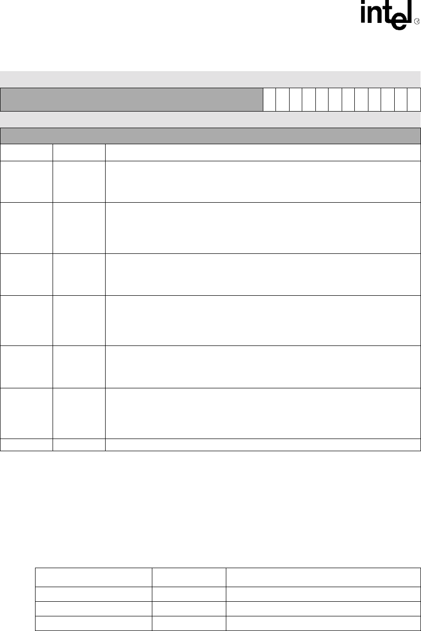
0h B010 0004 LCSR: LCD Status Register Read/Write and Read-Only
31 30 29 28 27 26 25 24 23 22 21 20 19 18 17 16 15 14 13 12 11 10 9 8 7 6 5 4 3 2 1 0
Reserved
OUU
OOU
OUL
OOL
IUU
IOU
IUL
IOL
ABC
BER
BAU
LDD
Reset 0 0 0 0 0 0 0 0 0 0 0 0 0 0 0 0 0 0 0 0 0 0 0 0 0 0 0 0 0 0 0 0
(Sheet 2 of 2)
Bits Name Description
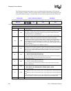
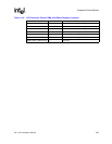
Table 11-10. LCD Controller Control, DMA, and Status Register Locations
Address Name Description
0hB010 0000 LCCR0 LCD controller control register 0
0hB010 0004 LCSR LCD controller status register 1
0hB010 0008 – 0h B010 000C — Reserved