


SA-1110 Developer’s Manual 377
Peripheral Control Module
11.12.11 SSP Data Register
The SSP data register (SSDR) is 16 bits wide and corresponds to the top and bottom entries of the
transmit and receive FIFOs, respectively. When SSDR is read, the bottom entry of receive FIFO is
accessed. As data is removed by the SSP’s receive logic from the incoming data frame, it is placed
into the top entry of the receive FIFO and is transferred down an entry at a time until it reaches the
last empty location within the FIFO. Data is removed by reading SSDR, which accesses the bottom
entry of the FIFO. After SSDR is read, the bottom entry is invalidated, and all remaining values
within the FIFO automatically transfer down one location.
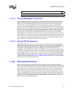
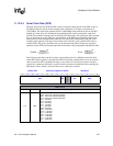
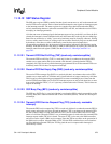
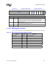
0h 8007 0064 SSP Control Register 1: SSCR1 Read/Write
15 14 13 12 11 10 9 8 7 6 5 4 3 2 1 0
Reserved ECS
SPH
SPO
LBM TIE RIE
0 0 0 0 0 0 0 0 0 0 ? ? ? ? ? ?
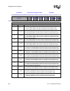
Bits Name Description
ORIE
Receive FIFO interrupt enable.
0 – Receive FIFO one- to two-thirds full or more condition does not generate an interrupt
(RFS bit ignored).
1 – Receive FIFO one- to two-thirds full or more condition generates an interrupt (state of
RFS sent to interrupt controller).
1TIE
Transmit FIFO interrupt enable.
0 – Transmit FIFO half-full or less condition does not generate an interrupt (TFS bit
ignored).
1 – Transmit FIFO half-full or less condition generates an interrupt (state of TFS sent to
interrupt controller).
2LBM
Loopback mode.
0 – Normal serial port operation enabled.
1 – Output of transmit serial shifter is connected to input of receive serial shifter internally
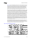
and control of TXD4, RXD4, SCLK, and SFRM pins is given to the PPC unit.
3SPO
Serial clock polarity.
0 – The inactive or idle state of SCLK is low.
1 – The inactive or idle state of SCLK is high.
4SPH
Serial clock phase.
0 – SCLK is in its inactive state one full cycle at the start of the frame and one-half cycle at
the end of the frame.
1 – SCLK is in its inactive state one-half cycle at the start of the frame and one full cycle at
the end of the frame.
5ECS
External clock select.
0 – Integrated clock generates the SSP serial clock and controls all timing.
1 – Clock input using GPIO pin 19 to drive the serial clock and all timing when serial rates
that are not a multiple of 3.6864 MHz are needed.
Note that bit 19 within GFAR and GPDR must be correctly configured within the system
control module.
15..6 — Reserved.