


378 SA-1110 Developer’s Manual
Peripheral Control Module
When SSDR is written, the topmost entry of the transmit FIFO is accessed. After a write, data is
automatically transferred down to the lowest location within the transmit FIFO, which does not
already contain valid data. Data is removed from the bottom of the FIFO one value at a time by the
transmit logic, is loaded into the transmit serial shifter, and then is serially shifted onto the TXD4
pin at the programmed bit rate.
When a data size of less than 16 bits is selected, the user should left justify data written to the
transmit FIFO. The transmit logic ignores the upper unused bits. Received data less than 16 bits is
automatically right justified in the receive buffer and unused bits are zero filled. When the SSP is
programmed for National Microwire frame format, the default size for transmit data is 8 bits (the
most significant byte is ignored) and the receive data size is controlled by the programmer.
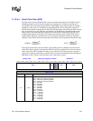
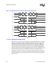
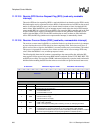
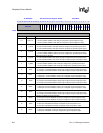
The following table shows the location of the SSP data register. Note that both FIFOs are cleared
when the SA-1110 is reset or by writing a zero to SSE (SSP disabled).
0h 8007 006C SSP Data Register: SSDR Read/Write
15 14 13 12 11 10 9 8 7 6 5 4 3 2 1 0
Bottom of Receive FIFO
Reset
? ? ? ? ? ? ? ? ? ? ? ? ? ? ? ?
Read Access
15 14 13 12 11 10 9 8 7 6 5 4 3 2 1 0
Top of Receive FIFO
Reset
? ? ? ? ? ? ? ? ? ? ? ? ? ? ? ?
Write Access
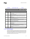
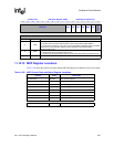
Bits Name Description
15..0 Data
Top/bottom of transmit/receive FIFO.
Read – Bottom of receive FIFO.
Write – Top of transmit FIFO.
Note: User should left justify data when SSP programmed for a data size less than 16 bits.
Top unused bits are ignored by transmit logic. Receive logic automatically right justifies
data and zero fills unused bits.