


372 SA-1110 Developer’s Manual
Peripheral Control Module
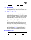
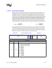
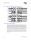
11.12.9 SSP Control Register 0
The SSP control register 0 (SSCR0) contains four different bit fields that control various functions
within the SSP.
11.12.9.1 Data Size Select (DSS)
The 4-bit data size select (DSS) field is used to select the size of the data transmitted and received by
the SSP. Data can be 4 to 16 bits in length. When data is programmed to be less than 16 bits, received
data is automatically right justified and the upper bits in the receive FIFO are zero filled by the
receive logic. Transmit data must be left justified by the user before being placed into the transmit
FIFO; however, the lower unused bits are ignored by the SSP’s transmit logic. Although it is possible
to program data sizes of 1, 2, and 3 bits, these sizes are reserved and produce unpredictable results in
the SSP. When National Microwire frame format is selected, this bit field selects the size of the
received data. Note that the size of the transmitted data is always 8 bits in this mode.
11.12.9.2 Frame Format (FRF)
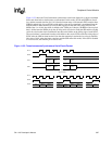
The 2-bit frame format (FRF) bit field is used to select which frame format to use: Motorola SPI
(FRF=00), Texas Instruments synchronous serial (FRF=01), or National Microwire (FRF=10). See
the preceding sections for a complete description of each frame format. Note that FRF=11 is
reserved and produces unpredictable results.
11.12.9.3 Synchronous Serial Port Enable (SSE)
The SSP enable (SSE) bit is used to enable and disable all SSP operation. When SSE=0, the SSP is
disabled; when SSE=1, it is enabled. Since the MCP and SSP both share the same pins, only one
can be enabled at a time. If the user enables both at the same time, the MCP has precedence and the
SSP remains disabled. However, both can be enabled when the SSP pin reassignment (SPR) bit
within the PPC unit is set, which assigns the SSP to GPIO pins.
When the SSP is disabled, all of its clocks are powered down to minimize power consumption. If
the MCP is also disabled, the TXD4, RXD4, SCLK, and SFRM pins can be used for
general-purpose input/output. See the Section 11.13, “Peripheral Pin Controller (PPC)” on
page 11-382 for a description of how to program the PPC unit to reassign the SSP’s pins and use
serial port 4’s pins as I/Os. Note that SSE is the only control bit within the SSP that is reset to a
known state. It is cleared to zero to ensure the SSP is disabled following a reset of the SA-1110.
When the SSE bit is cleared during active operation, the SSP is disabled immediately, causing the
current frame, which is being transmitted, to be terminated and control of serial port 4’s pins to be
given to the PPC unit. Clearing SSE resets the SSP’s FIFOs. However the SSP’s control and status
registers are not reset. The user must ensure these registers are properly reconfigured before
reenabling the SSP.