


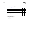
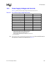


398 SA-1110 Developer’s Manual
AC Parameters
13.2 Model Considerations
The edge rates for the SA-1110 processor are such that the lumped load model presented above can
only be used for etch lengths up to one inch. Over one inch of etch, the signal is a transmission line
and needs to be modeled as such.
13.3 Memory Bus and PCMCIA Signal Timings
During production test, the SA-1110 is placed in test clock bypass mode by the assertion of the
TCKBYP pin. This mode (not intended for use by customers) bypasses the 3.686-MHz oscillator
and the main PLL and sources the processor clock from the TESTCLK pin. During this test mode,
all clocks on the SA-1110 are synchronous to TESTCLK. In this mode, the basic functionality of
the chip is tested and the pin timings relative to TESTCLK are measured. The ac parameters are
measured in this way for each available processor clock speed and supply voltage at which the
device is offered.
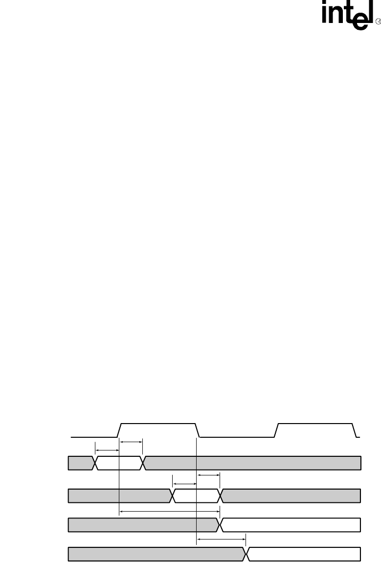
The ac specifications for the SA-1110 memory and PCMCIA interfaces are provided relative to the
memory clock. In the test clock bypass mode, memory clock is one-half the frequency of
TESTCLK. Under normal operation, memory clock is one-half the frequency of the processor
clock generated by the main PLL.
Even though this clock is not visible to the user, the required pin timing may be inferred through
these numbers. Input pins are specified by a required setup and hold to the memory clock. Outputs
are specified by a propagation delay from the edge of the memory clock where the drive starts to
the time the pin actually transitions. A 50-pF lumped load is assumed to be on each pin.
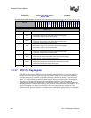
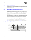
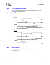
Figure 13-1 shows the memory bus ac timing definitions and Table 13-4 describes the ac timing
parameters.
Figure 13-1. Memory Bus AC Timing Definitions
A4776-01
Input hold from memory clock rise
Input setup to memory clock rise
Input hold from memory clock fall
Input setup to memory clock fall
Memory clock rise to output driven valid
Memory clock fall to output driven valid
Memory Clock
Memory Bus In
(B)
Memory Bus Out
(A)
Memory Bus Out
(B)
Memory Bus In
(A)