


SA-1110 Developer’s Manual 417
Boundary-Scan Test Interface
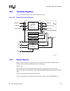
16.6 Test Data Registers
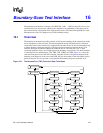
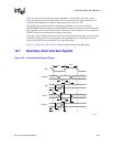
Figure 16-2 illustrates the structure of the boundary-scan logic.
Figure 16-2. Boundary-Scan Block Diagram
16.6.1 Bypass Register
Purpose: This is a single-bit register that can be selected as the path between TDI and TDO to
allow the device to be bypassed during boundary-scan testing.
Length: 1 bit
Operating Mode: When the BYPASS instruction is the current instruction in the instruction
register, serial data is transferred from TDI to TDO in the SHIFT-DR state with a delay of one TCK
cycle.
There is no parallel output from the bypass register.
A logic 0 is loaded from the parallel input of the bypass register in the CAPTURE-DR state.
A6831-01
BSINCELL
BSOUTCELL
BSOUTCELL
BSINENCELL
BSINCELL
BSOUTNENCELL
I/O
Cell
Intel
®
StrongARM*
SA-1110
Device ID Register
Bypass Register
Instruction Decoder
TDO
TDI
TMS
TCK
nTRST
Instruction Register
nTDOEN
Core Logic
TAP
Controller