


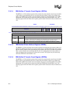
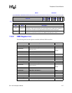
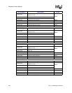

220 SA-1110 Developer’s Manual
Peripheral Control Module
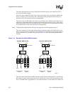
When the LCD controller is disabled, control of its pins is given to the peripheral pin controller
(PPC) to be used as general-purpose digital input/output pins that are noninterruptible. The LCD
controller’s pins include:
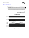
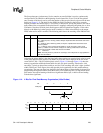
• LDD[7:0]
Data lines used to transmit either four or eight data values at a time to the LCD display. For
monochrome displays, each pin value represents a pixel; for passive color, groupings of three
pin values represent one pixel (red, green, and blue data values). In single-panel monochrome
mode, LDD[3:0] pins are used. For double-pixel data, single-panel monochrome, dual-panel
monochrome, single-panel color, and active color modes LDD[7:0] are used.
• GPIO[9:2]
When dual-panel color or 16-bit TFT operation is programmed, GPIO pins are used as the
additional, required LCD data lines to output pixel data to the screen.
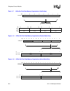
• L_PCLK
Pixel clock used by the LCD display to clock the pixel data into the line shift register. In
passive mode, pixel clock transitions only when valid data is available on the data pins. In
active mode, pixel clock transitions continuously and the ac bias pin is used as an output to
signal when data is available on the LCD’s data pins.
• L_LCLK
Line clock used by the LCD display to signal the end of a line of pixels that transfers the line
data from the shift register to the screen and increment the line pointers. Also, it is used by
TFT displays as the horizontal synchronization signal.
• L_FCLK
Frame clock used by the LCD displays to signal the start of a new frame of pixels that resets
the line pointers to the top of the screen. Also, it is used by TFT displays as the vertical
synchronization signal.
• L_BIAS
AC bias used to signal the LCD display to switch the polarity of the power supplies to the row
and column axis of the screen to counteract DC offset. In TFT mode, it is used as the output
enable to signal when data should be latched from the data pins using the pixel clock.
The pixel clock frequency is derived from the output of the on-chip PLL that is used to clock the
CPU (CCLK) and is programmable from CCLK/6 to CCLK/514. Each time new data is supplied to
the LCD data pins, the pixel clock is toggled to latch the data into the LCD display’s serial shifter.
The line clock toggles after all pixels in a line have been transmitted to the LCD driver and a
programmable number of pixel clock wait states have elapsed both at the beginning and end of
each line. In passive mode, the frame clock is asserted during the first line of the screen. In active
mode, the frame clock is asserted at the beginning of each frame after a programmable number of
line clock wait states occur. In passive display mode, the pixel clock does not transition when the
line clock is asserted. However, in active display mode, the pixel clock transitions continuously
and the ac bias bin is used as an output enable to signal when valid pixels are present on the LCD’s
data lines. In passive mode, the ac bias pin can be configured to transition each time a
programmable number of line clocks have elapsed to signal the display to reverse the polarity of its
voltage to counteract DC offset in the screen.
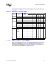
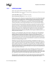
11.7.1 LCD Controller Operation
The LCD controller supports a variety of user-programmable options including display type and size,
frame buffer, encoded pixel size, and output data width. Although all programmable combinations are
possible, the selection of displays available within the market dictate which combinations of these
programmable options are practical. The type of external memory system implemented by the user