


SA-1110 Developer’s Manual 235
Peripheral Control Module
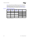
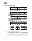
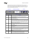
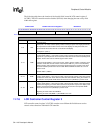
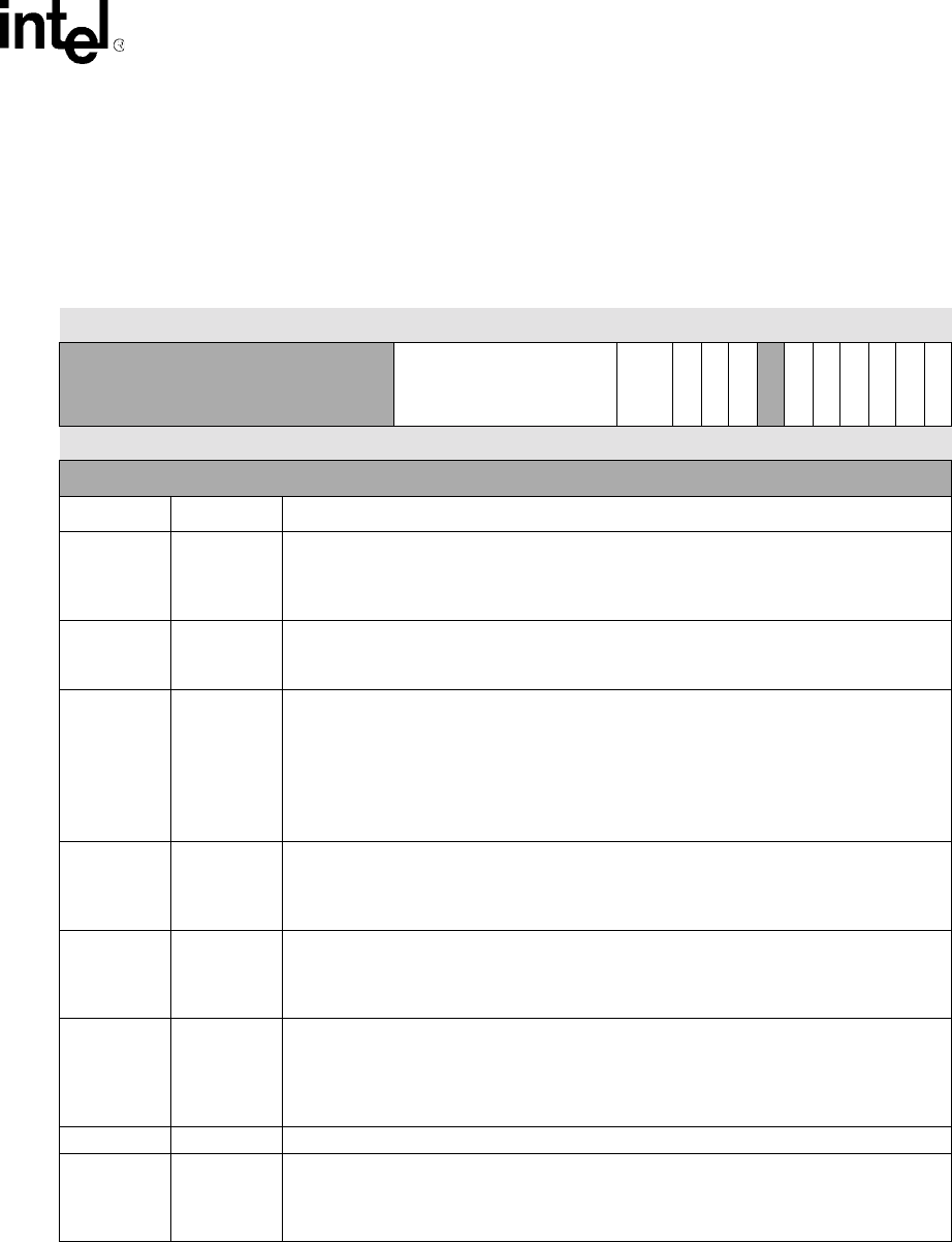
The following table shows the location of all 10 bit-fields located in LCD control register 0
(LCCR0). The user must program the control bits within all other control registers before setting
LEN=1 (a word write can be used to configure LCCR0 while setting LEN after all other control
registers have been programmed), and also must disable the LCD controller when changing the
state of any control bit within the LCD controller.
0h B010 0000 LCCR0: LCD Control Register 0 Read/Write
31 30 29 28 27 26 25 24 23 22 21 20 19 18 17 16 15 14 13 12 11 10 9 8 7 6 5 4 3 2 1 0
Reserved PDD
VSC
DPD
BLE
PAS
Reserved
ERM
BAM
LDM
SDS
CMS
LEN
Reset 0 0 0 0 0 0 0 0 0 0 0 0 0 0 0 0 0 0 0 0 0 0 0 0 0 0 0 0 0 0 0 0
(Sheet 1 of 2)
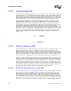
Bits Name Description
0LEN
LCD controller enable.
0 – LCD controller disabled. Control of L_PCLK, L_LCLK, L_FCLK, L_BIAS, and the
LDD[7:0] pins is given to the PPC unit to be used as general-purpose I/O pins.
1 – LCD controller enabled.
1CMS
Color/monochrome select.
0 – Color operation enabled.
1 – Monochrome operation enabled.
2SDS
Single-/dual-panel display select.
0 – Single-panel display enabled. LDD[3:0] used for monochrome, LDD[7:0] used for color.
1 – Dual-panel display enabled. LDD[7:0] used for monochrome, LDD[7:0] and GPIO[9:2]
used for color (user must also program GPDR and GAFR registers within the GPIO unit).
Note: SDS is ignored in active mode (PAS=1). For dual-panel operation, the user must
disable the LCD, set SDS, program the upper panel DMA base address, program the lower
panel DMA base address, and enable the LCD.
3LDM
LCD disable done mask.
0 – LCD disable done condition generates an interrupt (state of LDD status sent to the
interrupt controller).
1 – LCD disable done condition does not generate an interrupt (LDD status bit ignored).
4BAM
Base address update mask.
0 – Base address update condition generates an interrupt (state of BAU status sent to the
interrupt controller).
1 – Base address update condition does not generate an interrupt (BAU status bit ignored).
5ERM
Error mask.
0 – Bus error and FIFO over/underrun errors generate an interrupt (state of BER, IOL, IUL,
IOU, IUU, OOL, OUL, OUU status sent to the interrupt controller).
1 – Bus error and FIFO over/underrun errors do not generate an interrupt (BER, IOL, IUL,
IOU, IUU, OOL, OUL, OOU, OUU status bits ignored).
6 — Reserved.
7PAS
Passive/active display select.
0 – Passive or STN display operation enabled. Dither logic is enabled.
1 – Active or TFT display operation enable. Dither logic bypassed, pin timing changes to
support continuous pixel clock, output enable, VSYNC, HSYNC signals.