


SA-1110 Developer’s Manual 343
Peripheral Control Module
The MCP contains two pairs of transmit FIFOs and two pairs of receive FIFOs, one each for audio
and telecom data, totalling four separate 8-entry x 16-bit FIFOs. The MCP also contains a 21-bit
data register used to transmit codec register reads and writes, as well as another 21-bit register to
receive the results of codec register reads. Touch-screen and ADC conversions are triggered, the
digital I/O lines are controlled using codec register writes, and the converted data and the state of
digital I/O lines are accessed using a codec register read.
In SSP mode, serial port 4 controls full-duplex synchronous serial transfers between the SA-1110
and off-chip devices that support National Microwire, Texas Instruments synchronous serial, or the
Motorola SPI protocol. The SSP functions as a master only and communicates to the off-chip slave
device by driving a serial bit rate clock ranging from 7.2 kHz to 1.8432 MHz along with a frame
synchronization pulse to denote the start of each frame transfer, and supports any data format
between 4 and 16 bits. Transmit and receive data is stored/collected using two separate 8-entry x
16-bit FIFOs. MCP operation takes precedence over SSP operation. If use of both the MCP and
SSP is required at the same time, the user can configure the SSP to take over control of GPIO pins
10 through 13, and the MCP uses the serial port 4 pins for transmission.
The external pins dedicated to this interface are TXD4, RXD4, SCLK, and SFRM. If use of both
the MCP and SSP is not required and serial port 4 is disabled, control of these pins is given to the
peripheral pin controller (PPC) to be used to perform general-purpose input/output
(noninterruptible). See the section 11.13 on page 382 for a description of the programming and
operation of the PPC. The MCP operation takes precedence over the SSP if both units are enabled
(see section 11.12.1.6 on page 11-132). Both the MCP and SSP support word reads/writes of their
registers, and half-word DMA transfers to or from their FIFOs that are 16-bits wide.
11.12.1 MCP Operation
Following reset, both the MCP and SSP logic within serial port 4 is disabled and control of its pins
is given to the PPC, which configures all four pins as inputs. To enable MCP operation, the
programmer should first clear any interruptible status bits, which are set following the reset, by
writing a one to them. Next, the user should program the MCP control register with the desired
mode of operation using word writes, ensuring that the enable bit is programmed last. The user can
choose to either “prime” the audio and telecom transmit FIFOs, before enabling the MCP, by
writing up to eight 16-bit values each, or allow the FIFO service requests to interrupt the CPU or
trigger a DMA transfer to fill the FIFOs. Once the off-chip codec is programmed and data resides
within the bottom entries of the audio and/or telecom FIFOs, transmission/reception of data begins
on the transmit (TXD4) and receive (RXD4) pins, and is synchronously controlled by the serial
clock (SCLK) pin and a serial frame (SFRM) pin at an internally generated rate of 9.585 MHz or
11.981 MHz, or by an external clock input to GPIO21. The serial clock rate is selected by
programming a control bit. Note that the two internally generated SCLK rates are derived by first
multiplying the 3.6864-MHz on-chip oscillator by 13, then by dividing either by 5 (9.58464 MHz)
or by 4 (11.9808 MHz). Also note that an external clock input to GPIO21 can be used to drive the
MCP when a sample rate that is not a multiple of 3.6864 MHz is required.
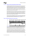
11.12.1.1 Frame Format
Each MCP data frame is 128 bits long and is divided into two subframes: 0 and 1. Subframe 0 is
used by the MCP to communicate data to and from the UCB1100, UCB1200, or UCB1300. The
timing of Subframe 1 is generated by the MCP, but the fields are not supported by the MCP.
After the MCP is enabled, SCLK begins to transition at the programmed clock rate and the start of the
first frame is signalled by pulsing the SFRM pin high for one SCLK period. The rising edge of SFRM
coincides with the rising edge of SCLK. The SFRM pulse causes the MCP to transfer any available