


312 SA-1110 Developer’s Manual
Peripheral Control Module
11.10.6.7 Transmit FIFO Interrupt Enable (TIE)
The transmit FIFO interrupt mask (TIE) bit is used to mask or enable the transmit FIFO service
request interrupt. When TIE=0, the interrupt is masked and the state of the transmit FIFO service
request (TFS) bit within HSSP status register 0 is ignored by the interrupt controller. When TIE=1,
the interrupt is enabled, and whenever TFS is set (one), an interrupt request is made to the interrupt
controller. Note that programming TIE=0 does not affect the current state of TFS or the transmit
FIFO logic’s ability to set and clear TFS; it only blocks the generation of the interrupt request.
Also note that TIE does not affect generation of the transmit FIFO DMA request, which is asserted
whenever TFS=1.
11.10.6.8 Address Match Enable (AME)
The address match enable (AME) bit is used to enable or disable the receive logic from comparing
the address programmed in the address match value (AMV) bit field to the address of all incoming
frames. When AME=1, data is stored in the receive FIFO only for those frames that have addresses
that match AMV and for any frame that contains an address containing all ones (11111111),
denoting a global address. For frames in which the address does not match, the data and CRC are
ignored and the receiver resumes hunting for a preamble. When AME=0, address values are not
compared and the data in every frame is stored in the receive FIFO. The following table shows the
location of the bits within HSSP control register 0. RXE and TXE are the only control bits that are
reset to a known state to ensure the HSSP is disabled following a reset of the SA-1110. The reset
state of all other control bits is unknown (indicated by question marks) and must be initialized
before enabling the HSSP. Note that the HSSP must be disabled (RXE=TXE=0) when changing the
state of bits 0 and 1, and bits 2 through 7 may be written while the HSSP is enabled to allow
various modes to be changed during active operation.
Note: A question mark (?) signifies that the Reset value of that bit is undefined when the processor has
completed its reset cycle.
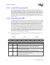
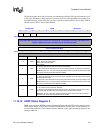
0h 8004 0060 HSCR0 Read/Write
7 6 5 4 3 2 1 0
AME TIE RIE RXE TXE TUS LBM
ITR
Reset
? ? ? 0 0 ? ? ?
(Sheet 1 of 2)
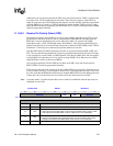
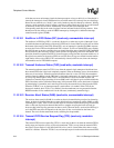
Bits Name Description
0ITR
IrDA transmission rate.
0 – 115.2 Kbps (selects HP-SIR modulation, enables the ICP’s UART engine).
1 – 4.0 Mbps (selects 4PPM modulation, enables the ICP’s HSSP engine).
1LBM
Loopback mode.
0 – Normal serial port operation enabled.
1 – Output of HSSP’s transmit serial shifter is connected to input of receive serial shifter
internally. Control of TXD2 and RXD2 pins is given to the PPC unit if ITR=1.
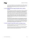
2TUS
Transmit FIFO underrun select.
0 – Transmit FIFO underrun causes CRC, stop flag, and SIP to be transmitted, and masks
transmit underrun interrupt generation (TUR ignored).
1 –Transmit FIFO underrun causes an abort to be transmitted, and generates an interrupt
(state of TUR sent to interrupt controller).