


SA-1110 Developer’s Manual 353
Peripheral Control Module
current state of ATS or the audio transmit FIFO logic’s ability to set and clear ATS; it only blocks
the generation of the interrupt request. Also note that ATE does not affect generation of the audio
transmit FIFO DMA request, which is asserted any time ATS=1.
11.12.3.9 Audio Receive FIFO Interrupt Enable (ARE)
The audio receive FIFO interrupt enable (ARE) bit is used to mask or enable the audio receive
FIFO service request interrupt. When ARE=0, the interrupt is masked, and the state of the audio
receive FIFO service request (ARS) bit within the MCP status register is ignored by the interrupt
controller. When ARE=1, the interrupt is enabled, and whenever ARS is set (one), an interrupt
request is made to the interrupt controller. Note that programming ARE=0 does not affect the
current state of ARS or the audio receive FIFO logic’s ability to set and clear ARS; it only blocks
the generation of the interrupt request. Also note that ARE does not affect generation of the audio
receive FIFO DMA request, which is asserted any time ARS=1.
11.12.3.10 Loopback Mode (LBM)
The loopback mode (LBM) bit is used to enable and disable the ability of the MCP’s transmit and
receive logic to communicate. When LBM=0, the MCP operates normally. The transmit and
receive data paths are independent and communicate via their respective pins. When LBM=1, the
output of the serial shifter (MSB) is directly connected to the input of the serial shifter (LSB)
internally and control of the TXD4, RXD4, SCLK, and SFRM pins are given to the peripheral pin
control (PPC) unit.
11.12.3.11 External Clock Prescaler (ECP)
The 2-bit external clock select (ECP) field is used to divide the clock input via GPIO pin 21 when
the external clock function is enabled. When ECS=1, ECP is decoded to divide the clock input on
the GPIO 21 pin by 1, 2, 3, or 4 before being used to drive the MCP’s frame rate. When ECP=00,
the input clock is divided by 1; when ECP=01, it is divided by 2; when ECP=10, it is divided by 3;
and when ECP=11, it is divided by 4. Note that the ECP bit field is ignored when the internal clock
(ECS=0) is used to drive the MCP’s frame rate. Also note that the resultant clock frequency after
the divide has taken place can be any value within the allowable frequency range of the UCB1x00
(upto12MHz).
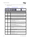
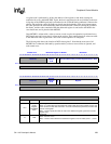
The following table shows the bit locations corresponding to the 11 different control bit fields
within the MCP control register. Note that the MCE bit is the only control bit that is reset to a
known state to ensure the MCP is disabled following a reset of the SA-1110. The reset state of all
other control bits is unknown (indicated by question marks) and must be initialized before enabling
the MCP. The user can program all 11 bit fields and enable the MCP using a single word write to
MCCR0. Writes to reserved bits are ignored and reads return zeros.