


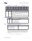
SA-1110 Developer’s Manual 143
Memory and PC-Card Control Module
To calculate the recommended BS_xx value for each address space (when MECR:FASTx=0):
divide the command width time (the greater of twIOWR and twIORD, or the greater of twWE and
twOE) by processor cycle time; divide by 2; divide again by 3 (number of BCLK’s per command
assertion); round up to the next whole number; and subtract 1. For example, for a processor cycle
time of 6.25 ns and an nIOWR command assertion time of 165 ns, the recommended setting for
BS_IO would be:
(165 / ( 2 x 3 x 6.25 ) ) = 4.4 or 5 after rounding up, 5 - 1 = 4
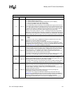
31 FAST1
Fast mode bit for access to slot 1 I/O, attribute, or memory.
If FAST1=1, the set-up time from address generated signals (A, nPREG, PSKTSEL and
nPCE) to initial assertion of the read or write strobe (nPWE, nPIOW, nPOE,ornPIOR)is
1*(BS_xx + 1) + 1 instead of the normal 3*(BS_xx + 1) + 1.
During I/O accesses, the nPCE set-up time is always reduced from these values by any
A-to-nIOIS16 delay.
The set-up time from address generated signals to the assertion of the read or write strobe
for the second half of a 16-bit access to 8-bit I/O is 2*(BS_xx + 1) instead of 1*(BS_xx + 1).
The duration of the read or write strobe remains 3*(BS_xx + 1), regardless of the value of
FAST1.
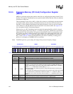
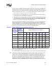
Table 10-5. BS_xx Bit Encoding
Bit Name Description
4..0 BS_xx 0b00000 – BCLK= 2 processor clocks (clk/2)
0b00001 – BCLK= 4 processor clocks
0b00010 – BCLK= 6 processor clocks
....
0b11101 – BCLK= 60 processor clocks
0b11110 – BCLK= 62 processor clocks
0b11111 – BCLK= 64 processor clocks
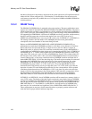
Table 10-6. BCLK Speeds for 160-MHz Processor Core Frequency
BS_xx BCLK Cycle Time–ns
0b00000 – Every 2 processor clocks (clk/2).
0b00001 – Every 4 processor clocks.
0b00010 – Every 6 processor clocks.
0b00011 – Every 8 processor clocks.
...
0b11111 – Every 64 processor clocks.
12.5
25
37.5
50
400
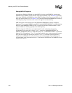
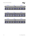
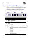
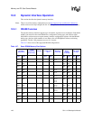
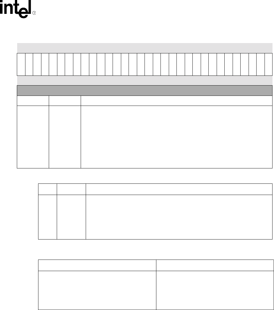
0h A000 0018 MECR Read/Write
31 30 29 28 27 26 25 24 23 22 21 20 19 18 17 16 15 14 13 12 11 10 9 8 7 6 5 4 3 2 1 0
FAST1
BSM1_4
BSM1_3
BSM1_2
BSM1_1
BSM1_0
BSA1_4
BSA1_3
BSA1_2
BSA1_1
BSA1_0
BSIO1_4
BSIO1_3
BSIO1_2
BSIO1_1
BSIO1_0
FAST0
BSM0_4
BSM0_3
BSM0_2
BSM0_1
BSM0_0
BSA0_4
BSA0_3
BSA0_2
BSA0_1
BSA0_0
BSIO0_4
BSIO0_3
BSIO0_2
BSIO0_1
BSIO0_0
Reset ? ? ? ? ? ? ? ? ? ? ? ? ? ? ? ? ? ? ? ? ? ? ? ? ? ? ? ? ? ? ? ?
(Sheet 2 of 2)
Bits Name Description