


SA-1110 Developer’s Manual 325
Peripheral Control Module
11.11 Serial Port 3 – UART
Serial port 3 is a general-purpose, full-duplex, universal asynchronous receiver/transmitter (UART)
that supports much of the functionality of the 16550 protocol. It can operate at baud rates from
56.25 bps to 230.4 Kbps. It supports 7 or 8 bits of data (odd, even, or no parity), one start bit, either
one or two stop bits, and can transmit a continuous break signal. An external clock can also be
input using GPIO pin 20 to synchronously sample and drive data on either edge of the clock as
programmed by the user. The external pins dedicated to this interface are TXD3 and RXD3. If use
of the UART is not required, these pins can be used by the peripheral pin controller (PPC) to
perform general- purpose input/output (noninterruptible).
An 8-entry x 8-bit FIFO is used to buffer outgoing data, and a 12-entry x 11-bit FIFO is used to
buffer incoming data (3 bits per entry are used to store framing, parity, and receive FIFO overrun
error flags for each character received). The FIFOs are filled or emptied using the DMA or the
CPU. An interrupt is generated when a framing, parity, or receiver overrun error is present within
the bottom four entries of the receive FIFO, when the transmit FIFO is half-empty or the receive
FIFO is one- to two-thirds full, when a begin and end of break is detected on the receiver, and when
the receive FIFO is partially full and the receiver is idle for three or more frame periods.
Modem control signals (RTS, CTS, DTR, and DSR) are not implemented in this block, but can be
implemented using the general-purpose I/O port (GPIO) pins. See Chapter 9, “System Control
Module”.
11.11.1 UART Operation
Following hardware reset, the UART is disabled, which causes the peripheral pin controller (PPC)
to assume control of the UART’s pins. Reset causes the PPC to configure all of the peripheral pins
as inputs, including the UART’s transmit (TXD3) and receive (RXD3) pins. Reset also causes the
UART’s transmit and receive FIFOs to be flushed (all entries invalidated). Before enabling the
UART, the user must first clear any writable or “sticky” status bits that are set by writing a one to
each bit. Next, the desired mode of operation is programmed in the control registers. At this point,
the user may “prime” the transmit FIFO by writing up to eight values, or the FIFO can remain
empty and the transmit FIFO DMA or interrupt request may be used to trigger its service when the
transmitter is enabled. When the UART is enabled, transmission and reception of data can begin on
the transmit (TXD3) and receive (RXD3) pins.
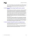
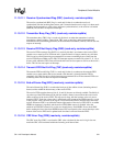
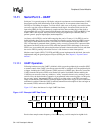
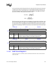
Figure 11-27 showstheformatofasingleUARTdataframe.
Figure 11-27. Example UART Data Frame
Start
Bit
Data0 Data1 Data2 Data3 Data4 Data5 Data6 Data7
Parity
Bit
Stop
Bit 1
Stop
Bit 2
TXD3 or RXD3 pin
Optional Optional
LSB MSB
Receive data sample counter frequency = 16x bit frequency, each bit sampled on eighth clock.