


344 SA-1110 Developer’s Manual
Peripheral Control Module
audio and/or telecom data from their respective transmit FIFOs to a 64-bit serial shifter, setting the
appropriate audio/telecom valid flags as well. If the codec control register contains valid data, the
register value and address are placed within the appropriate fields in the shifter, and the read/write bit
is configured to indicate which type of register access is to be made. For any field that does not have
valid data available, the previous value transmitted is used. As long as the MCP is enabled, data
frames are continuously transferred, even if no valid data is available for transmission. The format of
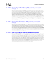
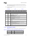
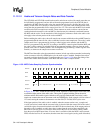
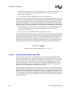
data transmitted and received in subframe 0 is shown in Figure 11-28. Note that the UCB1x00 and
the USB1200 data sheets use big-endian notation; little-endian notation is used in the following figure
to remain consistent with the rest of the SA-1110 specification.
Figure 11-28. MCP Frame Data Format
Both the MCP and the off-chip codec drive data on the rising edge of SCLK and latch data on its
falling edge. After SFRM is negated, subframe 0 begins and the data within the 64-bit shifter is
driven onto the TXD4 pin a bit at a time, starting with the MSB (bit 63). As each bit of data is
shifted onto the TXD4 pin from one side of the shifter, a bit is also shifted into the opposite end of
the shifter from the RXD4 pin. After 64 SCLK cycles elapse, all data within the shifter has been
transmitted, and the shifter contains the 64-bit receive data frame. The MCP takes the data from
each field and places it in its respective receive FIFO or data register. The next 64 SCLK cycles
make up subframe 1. When subframe 1 is active, the clocks to all MCP resources that are not
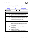
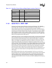
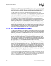
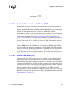
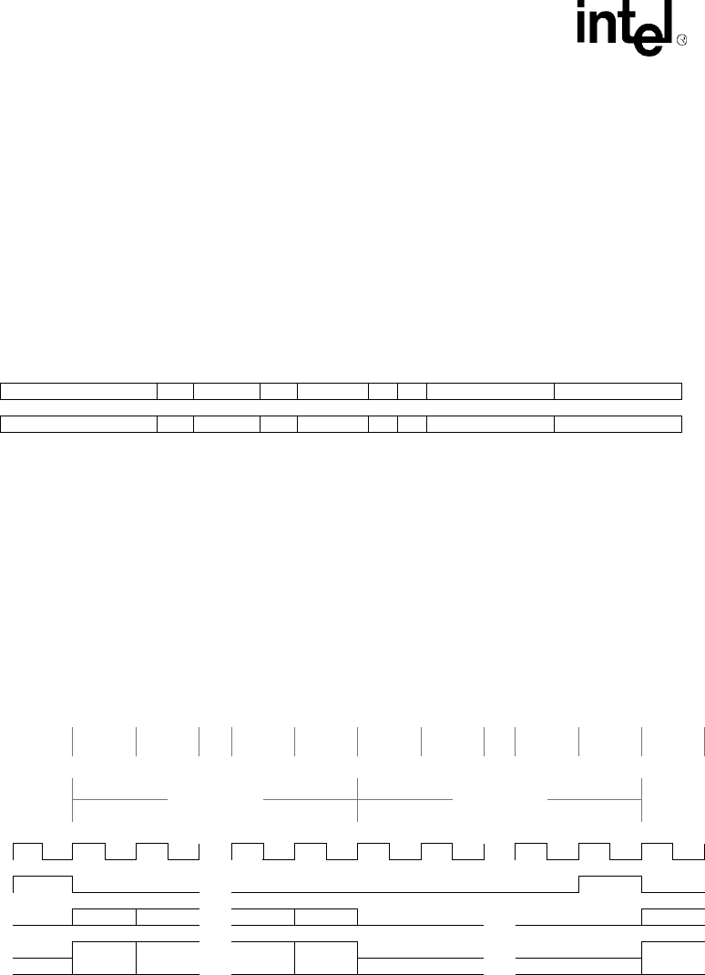
needed are turned off to conserve power. Figure 11-29 shows the pin timing of the MCP.
Figure 11-29. MCP Frame Pin Timing
Note that the transmit line is pulled low any time data is not being driven onto the pin. The
UCB1x00 have a programming option that allows them to either tri-state or drive the receive line
low when data is not being driven onto RXD4. As shown in Figure 11-29, MCP frames occur
back-to-back. The SFRM pin is pulsed high during the last clock (128th) of the frame to indicate
the start of a new frame the following SCLK period. Values contained within the transmit FIFOs
are loaded to the shift register on the rising edge of SFRM.
Bit
63 48 47 46 43 42 41 34 33 32
3
1
1
6
1
5
0
TX Audio Transmit Data 0 Address R/W 00000000 AV TV Telecom Transmit Data Control Register Write
RX Audio Receive Data 0 Address R/W 00000000 AV TV Telecom ReceiveData Control Register Read
AV – Audio Data Valid TV – Telecom Data Valid R/W – Write=1, Read=0 Address – Codec Register Address
Frame Clock
Count
1 2 ... 63 64 65 66 ... 127 128 1
Subframe
Subframe 0 Subframe 1
SCLK
... ...
SFRM
...
TXD4
Bit63 Bit62 ... Bit1 Bit0 ... Bit63
RXD4
Bit63 Bit62 ... Bit1 Bit0 ... Bit63