


SA-1110 Developer’s Manual 315
Peripheral Control Module
Additionally, the user must ensure that the PPC sleep state direction bit for TXD2 is inverted from
its normal value, if TXP=0 indicating inverted data. Thus if the user wishes to make TXD2 an
output in sleep mode, but TXP=0 indicating the output is inverted, the PPC should be programmed
such that PSDR 14=1. Likewise, if TXP=0 and the user wishes to make TXD2 an input in sleep
mode, the PPC should be programmed such that PSDR 14=0. If TXP=1 indicating true data, PSDR
should be programmed normally.
11.10.8.2 Receive Pin Polarity Select (RXP)
The receive pin polarity select (RXP) bit is used to select whether data input to the ICP’s receive
pin (RXD2) is viewed by the ICP as true or complemented. When RXP=0, data input from the
RXD2 pin is first inverted before being sent to either the UART (low-speed mode), HSSP
(high-speed mode), or PPC (GPIO input mode). When RXP=1, data input from the RXD2 pin is
treated as true data and is not inverted before being sent to either the UART, HSSP, or PPC. RXP is
initialized to 1 following reset such that input pin data defaults to true data.
Note that RXP affects the RXD2 pin during all modes of operation including HSSP, UART, and
PCC. The user should ensure that this bit is properly programmed when using serial port 2 for high-
or low-speed IrDA, normal UART, or GPIO operation. Note that for GPIO mode, the user needs to
configure RXP only when the pin is to be used as an input (PPDR 15=0). When used as a GPIO
output, RXP has no effect on the state of RXD2.
Also note that, unlike the TXP bit, RXP has no effect on the PPC sleep state direction bit for
RXD2. PSDR 15 should be programmed normally.
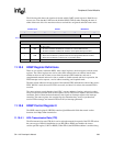
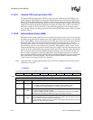
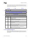
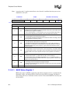
The following table shows the location of the bits within HSSP control register 2. Both bits are set
to one to ensure serial port 2’s pins default to normal “true” data operation following a reset of the
SA-1110. Note that the HSSP and UART must be disabled (RXE=TXE=0) when changing the state
of these bits. Also note that reads of reserved bits return zero and writes have no effect.
Note: A question mark (?) signifies that the Reset value of that bit is undefined when the processor has
completed its reset cycle.
0h 9006 0028 HSCR2 Read/Write
23 22 21 20 19 18 17 16
Reserved RXP TXP Reserved
Reset
0 0 0 0 1 1 0 0
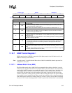
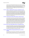
Bits Name Description
17..16 — Reserved.
18 TXP
Transmit pin polarity select.
0 – Data output from the HSSP, UART, or PPC is first inverted before being output to TXD2.
1 – Data output from the HSSP, UART, or PPC to TXD2 is true or non-inverted data.
19 RXP
Receive pin polarity select.
0 – Data input from RXD2 is first inverted before being used by the HSSP, UART, or PPC.
1 – Data input from RXD2 to the HSSP, UART, or PPC is true or non-inverted data.
23..20 — Reserved.