


SA-1110 Developer’s Manual 131
Memory and PC-Card Control Module
29..28 TDL21..0
Data input latch after CAS deassertion for bank 2/3.
For asynchronous DRAM, TDL is encoded with he number of CPU clocks between the
deassertion of nCAS/DQM and latching of read data.
For SDRAM, TDL is encoded with the CAS latency (external SDCLK delay between
reception of the READ command and latching of the data). The unit size for TDL is the
external SDCLK cycle: when SDRAM is run at half the memory clock frequency
(MDREFR:K2DB2 = 1), the delay is 2*TDL internal memory cycles.
00 – 0 clocks for asynchronous DRAM. Reserved (DO NOT USE) for SDRAM.
01 – 1clocklater
10 – 2 clocks later.
11 – 3 clocks later.
For SDRAM, the MDCASxx registers provide an option to add one-half memory clock of
CAS latency to TDL. See Section 10.3.3.2 for a detailed description. Chapter 13, “AC
Parameters” provides frequency-dependent guidelines for using the delayed latching
option.
31..30 TWR21..0
SDRAM write recovery (write data to precharge delay) for bank pair 2/3
For SDRAM only. TWR is encoded with the number of memory clocks to be added to the
minimum precharge delay that follows write transfers. The unit size for TWR is always the
internal memory cycle, even if SDRAM is run at half the memory clock frequency
(MDREFR:K2DB2 = 1).
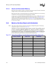
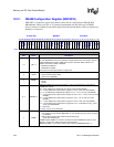
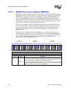
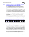
0h A000 0000 MDCNFG Read/Write
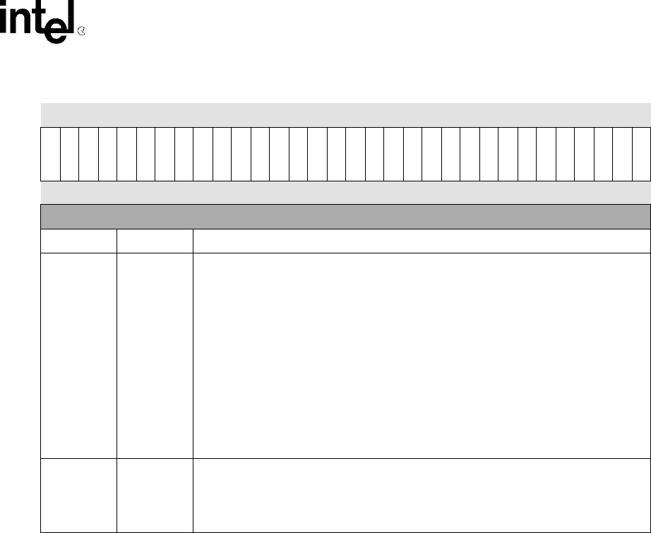
31 30 29 28 27 26 25 24 23 22 21 20 19 18 17 16 15 14 13 12 11 10 9 8 7 6 5 4 3 2 1 0
TWR21
TWR20
TDL21
TDL20
TRP23
TRP22
TRP21
TRP20
CDB22
DRAC22
DRAC21
DRAC20
DWID2
DTIM2
DE3
DE2
TWR01
TWR00
TDL01
TDL00
TRP03
TRP02
TRP01
TRP00
CDB20
DRAC02
DRAC01
DRAC00
DWID0
DTIM0
DE1
DE0
Reset ? ? ? ? ? ? ? ? ? ? ? ? ? ? 0 0 ? ? ? ? ? ? ? ? ? ? ? ? ? ? 0 0
(Sheet 4 of 4)
Bits Name Description