SA-1110 Developer’s Manual 153
Memory and PC-Card Control Module
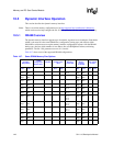
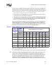
TDL2 field of MDCNFG. See Table 10-7 and Table 10-8 for a review of addressing, applicable to
all types of DRAM. The upper one or two bits of row address act as selects for SDRAM internal
banks.
Note: IMPORTANT ISSUE WHEN USING SDRAM WITH 103MHz SDCLK
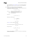
For correct operation of a 206MHz SA-1110 configured for 103MHz SDCLK operation, the choice
of SDRAM should not violate the following expression:
where: T
ac
= SDRAM access time from clk or, clk to data valid delay
T
sdis
= SA-1110 data input setup time to SDCLK rise
T
prop
= propagation delay due to board layout or trace routing
T
sdclk
=SA-1110SDCLKperiod
Solving for T
ac
:
SDCLK period = 1/SDCLK frequency:
or
From Table 13-3: SDCLK = 103MHz, delayed latching.
If any board related propagation delay is assumed to be no greater than 1 ns, then:
Evaluate the expression:
or
Therefore, your choice of SDRAM product must have a T
ac
value of 6ns or less to operate properly
at 206 MHz and 103MHz SDCLK.
T
ac
T
sdis
T
prop
++ T
sdclk
≤
T
ac
T
sdclk
≤ T
sdis
T
prop
––
T
sdclk
1cycle
103
6
×10 cycles()s⁄
------------------------------------------------
=
T
sdclk
9.7ns=
T
sdis
2.7ns=
T
prop
1ns≈
T
ac
9.7ns 2.7ns–1ns–≤
T
ac
6ns≤


