


390 SA-1110 Developer’s Manual
Peripheral Control Module
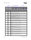
11.13.7 PPC Pin Flag Register
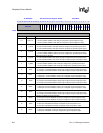
The PPC pin flag register (PPFR) is used to determine which peripherals are currently under the
control of the PPC unit. The eight read-only flags denote whether or not each of the peripherals
(except serial port 0) is enabled or is disabled and being controlled by the PPC. Note that serial
ports 1..3 contain individual enables for their transmit and receive serial engines. Thus, separate
flag bits exist for their transmit and receive pins. When a flag is set, it indicates that the
corresponding peripheral is disabled and is controlled by the PPC; when it is cleared, it indicates
that the peripheral is enabled and its pins are being used for serial transmission (serial ports 1..4) or
for LCD operation. Note that for reserved bits, writes are ignored and reads return zero. The
following table shows the location of each pin flag bit and to which peripheral pin it corresponds.
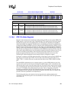
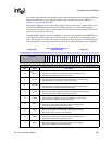
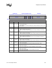
16 TXD3
Serial port 3: UART transmit sleep mode pin direction.
0 – Transmit pin configured as output and is driven low during sleep.
1 – Transmit pin configured as input during sleep.
17 RXD3
Serial port 3: UART receive sleep mode pin direction.
0 – Receive pin configured as output and is driven low during sleep.
1 – Receive pin configured as input during sleep.
18 TXD4
Serial port 4: MCP/SSP transmit sleep mode pin direction.
0 – Transmit pin configured as output and is driven low during sleep.
1 – Transmit pin configured as input during sleep.
19 RXD4
Serial port 4: MCP/SSP receive sleep mode pin direction.
0 – Receive pin configured as output and is driven low during sleep.
1 – Receive pin configured as input during sleep.
20 SCLK
Serial port 4: MCP/SSP serial clock sleep mode pin direction.
0 – Serial clock pin configured as output and is driven low during sleep.
1 – Serial clock pin configured as input during sleep.
21 SFRM
Serial port 4: MCP/SSP serial frame sleep mode pin direction.
0 – Serial frame pin configured as output and is driven low during sleep.
1 – Serial frame pin configured as input during sleep.
31..22 — Reserved.
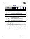
0h 9006 000C
PPC Pin Sleep Mode Direction
Register: PSDR
Read/Write
31 30 29 28 27 26 25 24 23 22 21 20 19 18 17 16 15 14 13 12 11 10 9 8 7 6 5 4 3 2 1 0
Reserved
SFRM
SCLK
RXD4
TXD4
RXD3
TXD3
RXD2
TXD2
RXD1
TXD1
L_BIAS
L_FCLD
L_LCLK
L_PCLK
LDD 7
LDD 6
LDD 5
LDD 4
LDD 3
LDD 2
LDD 1
LDD 0
0 0 0 0 0 0 0 0 0 0 1 1 1 1 1 1 1 1 1 1 1 1 1 1 1 1 1 1 1 1 1 1
(Sheet 2 of 2)
Bits Name Description