


SA-1110 Developer’s Manual 145
Memory and PC-Card Control Module
15 RL0
RAS latency for bank pair 0/1.
It is the RAS-to-CAS delay (number of external SDCLK cycles between ACT command and
READ command). The unit size for RL0 is the external SDCLK cycle: when SMROM is run
at half the memory clock frequency (MDREFR:K0DB2 = 1), the delay is 2*RL0 internal
memory cycles.
See Section 10.4.1 for description of the software sequence required whenever changing
the RAS latency.
0 - 1 clock.
1 - 2 clock.
Hardware or sleep reset forces RL0=1. If SMROM_EN=1, RL0 must be maintained at this
value to avoid a mismatch in RAS latency between the SA-1110 and boot SMROM following
a subsequent hardware or sleep reset.
17..16 SM3..2
SMROM enables for bank 3 (bit 17) and bank 2 (bit 16).
0 - Bank is not SMROM enabled.
1 - Bank is SMROM enabled.
19..18 — Reserved.
22..20 RA2 2..0
SMROM row address bit count for bank pair 2/3.
0xx - Reserved.
100 - 13 row address bits, supports 13x11, 13x10, 13x9, 13x8.
101 - Reserved.
11x - Reserved.
See Table 10-8 for a description of DRAM or SMROM row/column address multiplexing.
27..23 — Reserved.
30..28 CL2 2..0
CAS latency for bank pair 2/3.
It is the number of external SDCLK cycles between reception of the READ command and
latching of the data. The unit size for CL2 is the external SDCLK cycle: when SMROM is
run at half the memory clock frequency (MDREFR:K0DB2 = 1), the delay is 2*CL2 internal
memory cycles.
000 - Reserved.
001 - 2 clocks.
010 - 3 clocks.
011-4clocks.
100 - 5 clocks.
101 - 6 clocks.
110-7clocks.
111 - Reserved.
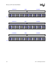
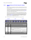
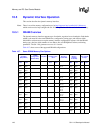
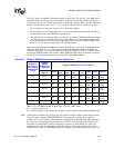
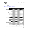
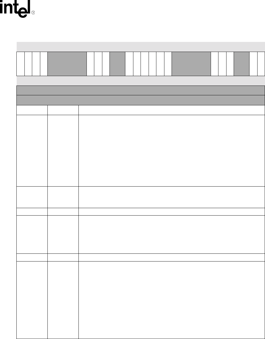
0h A000 0030 SMCNFG Read/Write
31 30 29 28 27 26 25 24 23 22 21 20 19 18 17 16 15 14 13 12 11 10 9 8 7 6 5 4 3 2 1 0
RL2
CL22
CL21
CL20
Reserved
RA22
RA21
RA20
Reserved
SM3
SM2
RL0
CL02
CL01
CL00
Reserved
RA02
RA01
RA00
Reserved
SM1
SM0
Reset ? ? ? ? ? ? ? ? ? ? ? ? ? ? 0 0 1 1 0 0 ? ? ? ? ? 1 0 0 ? ? 0 *
* Upon hardware or sleep reset, SM0 is set to the value of the SMROM_EN pin.
(Sheet 2 of 3)
Bits Name Description