


234 SA-1110 Developer’s Manual
Peripheral Control Module
packed into half-words starting with the most significant half-word. Note that BLE does not affect
the ordering of the 4-bit red/green/blue bit fields, the 4-bit monochrome field within each 16-bit
palette entry, or the 2-bit pixel bit size (PBS) field contained with palette entry 0.
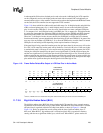
11.7.3.9 Double-Pixel Data (DPD) Pin Mode
The double-pixel data (DPD) pin mode bit selects whether four or eight data pins are used to output
pixel data to the LCD screen in single-panel monochrome mode. When DPD=0, LDD[3:0] pins are
used to output 4-pixel values each pixel clock transition; when DPD=1, LDD[7:0] pins are used to
output 8-pixel values each pixel clock. See Table 11-8 “Color/Gray-Scale Intensities and
Modulation Rates” on page 11-227 and Figure 11-8 “Frame Buffer/Palette Bits Output to LCD
Data Pins in Active Mode” on page 11-233 for a comparison of how the LCD’s data pins are used
in each of its display modes. Note that DPD does not affect dual-panel monochrome mode nor any
of the color modes.
11.7.3.10 Vertical Slant Line Correction (VSC)
See description of bits 11 and 10 in the table, “LCCR0: LCD Control Register 0”. Values other than
reset are not typically required. However, values other than reset can provide subjective
improvement in certain cases where a user experiences “vertical slant line flickering/ghosting”.
Values other than reset (patterns 1-3) have to be determined by a users experimentation with a
particular design. No guidance for experimentation will be provided here.
11.7.3.11 Palette DMA Request Delay (PDD)
The 8-bit palette DMA request delay (PDD) field is used to select the minimum number of memory
controller clock cycles (half the frequency of the CPU clock) to wait between the servicing of each
DMA request issued while the on-chip palette is loaded. When the palette is loaded at the beginning
of every frame, either 32 or 512 bytes of data must be accessed by the LCD’s DMA. Since the LCD’s
DMA is the highest priority master on the ARM system bus, other masters (such as the CPU) will be
denied access to the bus and may be starved. Using PDD allows other masters to gain access of the
bus in between palette DMA loads, so that they are not locked from accessing the bus for an
unacceptable period of time. Note that PDD does not apply to normal input FIFO DMA requests for
frame buffer information since these DMA requests do not occur back-to-back. The input FIFO DMA
request rate is a function of the rate at which pixels are displayed on the screen.
After a palette DMA burst cycle has completed, the value contained within PDD is loaded to a
down counter that disables the palette from issuing another DMA request until the counter
decrements to zero. This counter ensures that the LCD’s DMA does not fully consume the
bandwidth of the SA-1110’s system bus. Once the counter reaches zero, any pending or future
DMA requests by the palette cause the DMA to arbitrate for the ARM system bus (ASB). Once the
DMA burst cycle has completed, the process starts over and the value in PDD is loaded to the
counter to create another wait state period, which disables the palette from issuing a DMA request.
PDD can be programmed with a value that causes the FIFO to wait between 0 to 255 memory clock
cycles after the completion of one DMA request to the start of the next request. When PDD=8’h00,
the FIFO DMA request delay function is disabled. Note that waitstates are not inserted between
DMA burst cycles that are used to fill the input FIFO with pixel data.