


SA-1110 Developer’s Manual 113
System Control Module
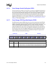
9.5.7.6 Power Manager Scratch Pad Register (PSPR)
The power manager also contains a 32-bit register to save processor configuration information in
any format the user desires. The power manager scratch pad register (PSPR) is a holding register
that is powered by the VDDx power supply pins and is never reset (only configured via writes).
Any value can be written to it while in run mode. The value remains intact while in sleep mode,
and can be read once sleep mode is exited. The user may use the register value to represent
processor configuration prior to sleep mode invocation. (The 32 bits can represent encoded
configuration information or can act as a pointer to ROM where a configuration table is kept.) The
PSPR is a simple read/write register. See the Section 9.5.8, “Power Manager Register Locations”
on page 9-114 for its physical address.
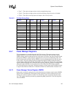
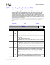
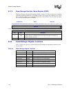
9.5.7.7 Power Manager GPIO Sleep State Register (PGSR)
The GPIO sleep state register (PGSR) allows the user to select the output state of each GPIO pin
when the SA-1110 goes into sleep mode. When a transition to sleep is required (either through
software or through the assertion of the BATT_FAULT or VDD_FAULT pins), the contents of the
PGSR is loaded into the GPIO output data register. [This register is normally controlled by
software through the GPSR (set) and GPCR (clear) registers]. Only pins already configured as
outputs will reflect the new state; however, all 28 bits of the output register are loaded. After the
SA-1110 reenters the run mode from sleep, these GPIO pins retain their programmed sleep state
until changed by writing ones to the GPSR or GPCR registers; question marks indicate that the
values are unknown at reset. If a pin direction is switched from an input to an output, the last
contents of the register will be driven onto the pin.
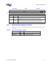
0h 9002 0018 PGSR Read/Write
31 30 29 28 27 26 25 24 23 22 21 20 19 18 17 16 15 14 13 12 11 10 9 8 7 6 5 4 3 2 1 0
Reserved
SS27
SS26
SS25
SS24
SS23
SS22
SS21
SS20
SS19
SS18
SS17
SS16
SS15
SS14
SS13
SS12
SS11
SS10
SS9
SS8
SS7
SS6
SS5
SS4
SS3
SS2
SS1
SS0
Reset 0 0 0 0 ? ? ? ? ? ? ? ? ? ? ? ? ? ? ? ? ? ? ? ? ? ? ? ? ? ? ? ?
Bits Name Description
nSSn
Sleep state of GPIO n (where n = 0 through 27)
0 – This pin is driven to a zero during the transition to sleep (if programmed as an output).
1 – This pin is driven to a one during the transition to sleep (if programmed as an output).
31..28 — Reserved