


296 SA-1110 Developer’s Manual
Peripheral Control Module
11.9.1.1 Simultaneous Use of the UART and GPCLK
Serial port 1 contains a control bit to select which serial protocol to use: GPCLK or UART. Note
that the two protocols cannot be combined at the same time (GPCLK transmit and UART receive).
However, since the GPCLK and UART are fully independent blocks, a mode is supported that
allows the user to enable the GPCLK using serial port 1’s pins (TXD1 and RXD1).
The UART is enabled using two GPIO pins (GPIO<14> for transmit and GPIO<15> for receive
operation). This mode is enabled by setting the UART pin reassignment (UPR) control bit within
the peripheral pin controller (PPC). For more information, see Section 11.13. Note that when this
mode is enabled, serial port 1’s control bit, which selects GPCLK versus UART operation, is
ignored and serial port 1 defaults to GPCLK mode.”
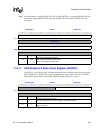
11.9.2 GPCLK Control Register 0
GPCLK control register 0 (GPCLKR0) contains 3 bit fields that control various functions within the
GPCLK.
11.9.2.1 GPCLK/UART Select (SUS)
The GPCLK/UART select (SUS) bit is used to select whether serial port 1 is used for GPCLK or
UART operation. When SUS=0, GPCLK operation is selected. When SUS=0 control of the
transmit pin (TXD1) is given to the PPC unit; when SUS=0 control of the receive pin (RXD1) is
given to the PPC unit. When SUS=1, UART operation is selected and the state of all remaining
GPCLK register bits is ignored (remaining unchanged) and control of the TXD1 and RXD1 pins is
given to the UART. See the Section 11.11, “Serial Port 3 – UART” on page 11-325 for a
description of the programming and operation of serial port 1 as a UART. The SUS bit is the only
bit within the control register that is reset, placing serial port 1 into GPCLK mode while disabling
the transmitter and receiver.
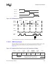
11.9.2.2 Sample Clock Enable (SCE)
The sample clock enable (SCE) bit is used to enable or disable driving or receiving a clock using
GPIO pin 16. When SCE=0, the sample clock is disabled. When SCE=1, the sample clock is
enabled.
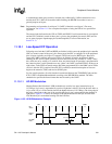
11.9.2.3 Sample Clock Direction (SCD)
When the sample clock function is enabled (SCE=1), the sample clock direction (SCD) bit is used
to select whether the sample clock is an input from or an output to GPIO pin 16. When SCD=0, the
sample clock is input using GPIO pin 16 and is not used. When SCD=1, the sample clock, which is
generated within the GPCLK unit (the clock that is output after dividing the 3.6864-MHz reference
by the programmable BRD field), is output to GPIO pin 16 in frequency ranging from 900 Hz to
3.6864 MHz.
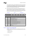
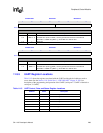
The following table shows the location of all bit fields located in GPCLK control register 0
(GPCLKR0). The GPCLK must be disabled (SUS=0) when changing the state of any bit within
this register.