


228 SA-1110 Developer’s Manual
Peripheral Control Module
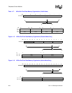
GPIO[9:2] and LDD[7:0]. In monochrome dual-panel mode, the pixels for the upper half of the
screen are driven onto LDD[3:0] and the lower half to LDD[7:4]. In color dual-panel mode, the
upper panel pixels are driven onto LDD[7:0] and the lower panel pixels to GPIO[9:2]. Note that for
a 4-bit wide bus, data is output via the LDD[3:0] pins and the LCD[7:4] pins are held low by the
LCD controller. The user cannot use this pins as GPIOs in this mode. However, for a 12-bit wide
bus, the user is free to use GPIO[9:6] as general- purpose I/O signals.
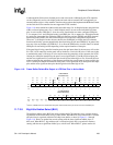
When an entire line of pixels has been output to the LCD controller screen, the line clock pin (L_LCLK)
is toggled. Likewise, when an entire frame of pixels has been output to the LCD controller screen, the
frame clock pin (L_FCLK) is toggled. To prevent a DC charge from building within a passive display,
its power and ground supplies must be switched periodically. The LCD controller signals the display to
switch the polarity by toggling the ac bias pin (L_BIAS). The user can control the frequency of the bias
pin by programming the number of line clock transitions between each toggle.
When active display mode is enabled, the timing of the pixel, line, and frame clocks and the ac bias
pin changes. The pixel clock transitions continuously in this mode as long as the LCD is enabled. The
ac bias pin functions as an output enable. When it is asserted, the display latches data from the LCD’s
pins using the pixel clock. The line clock pin is used as the horizontal synchronization signal
(HSYNC) and the frame clock as the vertical synchronization signal (VSYNC). The timing of the line
and frame clock pins is programmable to support both passive and active mode. Programming
options include: wait state insertion both at the beginning and end of each line and frame; pixel clock;
line clock; frame clock; output enable signal polarity; and frame clock pulse width.
When the LCD controller is disabled, control of all 12 of its pins is relinquished to the peripheral pin
controller (PPC) unit to be used as general-purpose digital I/O pins that are noninterruptible. See the
section 11.13 on page 382 for a description of the programming and operation of the PPC unit.
11.7.2 LCD Controller Register Definitions
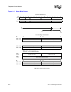
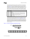
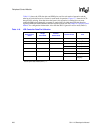
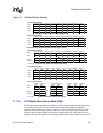
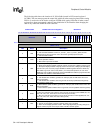
The LCD controller contains four control registers, four DMA address registers, and one status
register. The control registers contain bit fields to enable and disable the LCD controller; to define
the height and width of the screen being controlled; and to indicate single- versus dual-panel
display mode, color versus monochrome mode, passive versus active display, polarity of the
control pins, pulse width of the line and frame clocks, pixel clock and ac bias pin frequency. AC
bias pin toggles per interrupt the number of waitstates to insert before and after each line, after each
frame, and various interrupt masks. An additional control field exists to tune the DMA’s
performance based on the type of memory system in which the SA-1110 is used. This field controls
the placement of a minimum delay between each LCD DMA request to ensure enough bus
bandwidth is given to other ARM system bus masters for accesses.
The DMA address registers are used to define the base physical addresses of the off-chip frame
buffers and to which physical address the DMA is currently pointing. Both of these registers exist for
DMA channels 1 and 2.
The status registers contain bits that signal input and output FIFO overrun and underrun errors,
DMA bus errors, when the DMA base address can be reprogrammed, when the last active frame
has completed after the LCD is disabled, and each time the ac bias pin has toggled a programmed
number of times. Each of these hardware-detected events signals an interrupt request to the
interrupt controller.