


SA-1110 Developer’s Manual 425
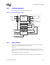
Boundary-Scan Test Interface
NOTES:
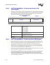
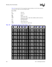
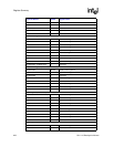
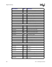
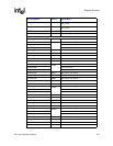
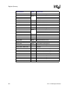
1. The Boundary Scan (BS) numbers are listed in order from the first BS latch after the TDI input pin. Thus, for
a given BS pattern, the first bit input will land in the 292nd BS latch and the last bit will land in the first BS
latch.
2. BS latch 80 controls the tristate enable of the D[31:0] pins. A “1” in latch 80 will tristate the D[31:0] pins.
3. BS latch 83 controls the tristate enable for output pin SDCLK 1. A “1” in latch 83 will tristate SDCLK 1.
4. BS latch 218 controls the tristate enable of nWE, nOE, nSDRAS, nSDCAS, nRAS 0, nCAS[3:0], and A[25:0].
A “1” in latch 218 will tristate these pins.
5. The output enable latches for UDC- and UDC+, 265 and 269, will tristate the outputs when a “1” is latched in.
6. For all other output or in/out pins, a “0” in the output enable latch will tristate the output in.
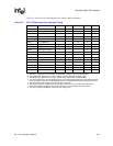
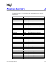
281 TXD_2 EN qjtena OEL 287 TXD_3 EN qjtena OEL
282 TXD_2 OUT qjto OCL 288 TXD_3 OUT qjto OCL
283 TXD_2 IN qjti ICL 289 TXD_3 IN qjti ICL
284 RXD_3 EN qjtena OEL 290 nRESET IN qjti ICL
285 RXD_3 OUT qjto OCL 291 nRESET_OUT OUT qjto OCL
286 RXD_3 IN qjti ICL 292 ROM_SEL IN qjti ICL
to TDO
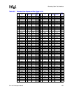
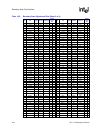
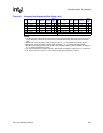
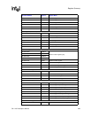
Table 16-2. Boundary-Scan Signals and Pins (Sheet 4 of 4)
No. Pin Type BS Cell
BS
Function
Guard
Value
EX
No. Pin Type BS Cell
BS
Function
Guard
Value
EX