


SA-1110 Developer’s Manual 371
Peripheral Control Module
11.12.7.4 CPU and DMA Register Access Sizes
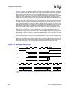
Bit positioning, byte ordering, and addressing of the SSP are described in terms of little endian
ordering. All SSP registers are 16-bits wide and are located in the least significant half-word of
individual words. The ARM peripheral bus does not support byte or half-word operations. All
reads and writes of the SSP by the CPU should be word wide. Two separate dedicated DMA
requests exist for both the transmit and the receive FIFO. If the DMA controller is used to service
the transmit and/or receive FIFOs, the user must ensure the DMA is properly configured to perform
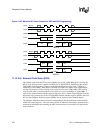
half-word wide accesses, using four half-words per burst (half the size of the FIFOs). Byte-wide
DMA accesses for data widths of 4..8 bits are not permitted. For all data sizes 4..16 bits, the user
must left-justify the data within each individual half-word in external memory for the DMA,
starting with the most significant bit. Likewise, when using programmed I/O to service the SSP’s
transmit FIFO, the user must also left-justify the data written or read to/from the data register. Note
that a separate set of registers also exist to configure MCP operation. See the following sections for
a full description of programming and operation of serial port 4 as an MCP, a summary of serial
port 4’s MCP registers, and for a summary of its SSP registers.
11.12.7.5 Alternate SSP Pin Assignment
If the SSP and MCP both need to be used at the same time, general-purpose I/O pins 10 through 13
(GPIO 10-13) can be reassigned by programming the PPC pin assignment register (PPAR). This
allows the MCP dedicated use of the four pins assigned to serial port 4, and the SSP dedicated use of
the GPIO pins. When the SSP pin reassignment (SPR) bit is set in PPAR, the following pin
assignments are made: GPIO 10 is used for transmit, GPIO 11 for receive, GPIO 12 for serial clock,
and GPIO 13 for serial frame. Note that the user must also set bits 10 through 13 in the GPIO alternate
function register (GAFR) as well as set bits 10, 12, and 13 and clear bit 11 in the GPIO pin direction
register (GPDR). Once the reassignment is made, these pins are no longer usable by the GPIO unit.
See the Section 9.1, “General-Purpose I/O” on page 9-73 for a description of how to program the
system control module and the Section 11.13, “Peripheral Pin Controller (PPC)” on page 11-382 for
a description of how to program the PPC unit.
11.12.8 SSP Register Definitions
There are four registers within the SSP: two control registers, one data register, and one status
register. The control registers are used to program the baud rate, data length, and frame format, and
to select whether the CPU or DMA is used to service the SSP, and to enable/disable operation. The
data register is 16 bits and addresses both the transmit and receive buffers. A read accesses the
receive buffer; a write accesses the transmit buffer. Note that these are two physically separate
buffers to allow full-duplex transmission. The status register contains bits that signal an overrun
error, a transmit buffer service request, and a receive buffer service request. Each of these status
conditions signal an interrupt request to the interrupt controller. The status register also flags when
the SSP is actively transmitting data, when the transmit FIFO is not full, and when the receive
FIFO is not empty (no interrupt generated).
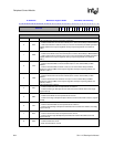
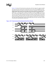
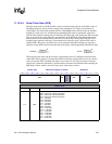
15-Bit Data 0
16-bit Data