


236 SA-1110 Developer’s Manual
Peripheral Control Module
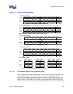
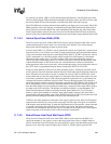
11.7.4 LCD Controller Control Register 1
LCD controller control register 1 (LCCR1) contains four bit fields that are used as modulus values
for a collection of down counters, each of which performs a different function to control the timing
of several of the LCD’s pins.
8BLE
Big/little endian select.
0 – Little endian operation is selected, half-word palette buffer data is packed into individual
words of memory starting with the least significant half-word, and frame buffer pixel data is
packed into individual words of memory starting with the least significant nibble, byte, or
half-word.
1 – Big endian operation is selected, half-word palette buffer data is packed into individual
words of memory starting with the most significant half-word, and frame buffer pixel data is
packed into individual words of memory starting with the most significant nibble, byte, or
half-word.
9DPD
Double-pixel data pin mode.
0 – In single-panel monochrome operation, four pixels are presented to LDD[3:0] each
pixel clock.
1 – In single-panel monochrome operation, eight pixels are presented to LDD[7:0] each
pixel clock.
Note: This bit is ignored in all other modes of operation except for single-panel
monochrome.
11..10 VSC
Vertical slant line correction.
Bits:11 10
00– Values after reset
Vertical slant correction pattern 0, modulation rate is 4/15 for intensity value 3 and
11/15 for intensity value 11
01– Vertical slant correction pattern 1, modulation rate is 4/15 for intensity value 3 and
11/15 for intensity value 11
10– Vertical slant correction pattern 2, modulation rate is 4/15 for intensity value 3 and
11/15 for intensity value 11
11– Vertical slant correction pattern 3, modulation rate is 6/15 for intensity value 3 and
9/15 for intensity value 11
19..12 PDD
Palette DMA request delay.
Value (from 0 to 255) used to specify the number of memory controller clocks (half the
speed of the CPU clock). The on-chip palette DMA request should be disabled after each
DMA transfer to the palette. The clock count starts after the last write of each burst cycle.
While the counter is decrementing, all DMA requests from the palette are masked. When
the counter reaches zero, any pending or subsequent DMA requests are allowed to
generate a 4-word burst. Programming PDD=8h’00 disables this function.
31..20 — Reserved.
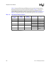
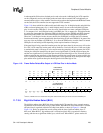
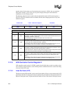
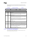
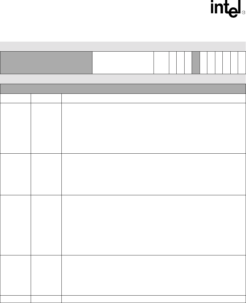
0h B010 0000 LCCR0: LCD Control Register 0 Read/Write
31 30 29 28 27 26 25 24 23 22 21 20 19 18 17 16 15 14 13 12 11 10 9 8 7 6 5 4 3 2 1 0
Reserved PDD
VSC
DPD
BLE
PAS
Reserved
ERM
BAM
LDM
SDS
CMS
LEN
Reset 0 0 0 0 0 0 0 0 0 0 0 0 0 0 0 0 0 0 0 0 0 0 0 0 0 0 0 0 0 0 0 0
(Sheet 2 of 2)
Bits Name Description