


244 SA-1110 Developer’s Manual
Peripheral Control Module
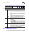
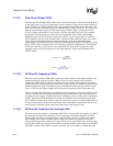
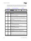
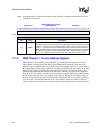
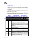
The following table shows the location of the seven different bit fields located in LCD controller
control register 3 (LCCR3). The LCD controller must be disabled (LEN=0) when changing the state
of any field within this register. Note that writes to reserved bits are ignored and reads return zeros.
0h B010 0028 LCCR3: LCD Control Register 3 Read/Write
31 30 29 28 27 26 25 24 23 22 21 20 19 18 17 16 15 14 13 12 11 10 9 8 7 6 5 4 3 2 1 0
Reserved
OEP
PCP
HSP
VSP
API ACB PCD
Reset
0 0 0 0 0 0 0 0 0 0 0 0 0 0 0 0 0 0 0 0 0 0 0 0 0 0 0 0 0 0 0 0
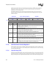
Bits Name Description
7..0 PCD
Pixel clock divisor.
Value (from 1 to 255). Used to specify the frequency of the pixel clock based on the CPU
clock (CCLK) frequency. Pixel clock frequency can range from CCLK/6 to CCLK/514.
Pixel Clock Frequency = CCLK/2(PCD+2).
Note that PCD must be programmed with a value of 1 or greater (PCD = 8’h00 is illegal).
15..8 ACB
AC bias pin frequency.
Value (from 1 to 256). Used to specify the number of line clocks to count before
transitioning the ac bias pin in passive mode (PAS=0). This pin is used to periodically invert
the polarity of the power supply to prevent DC charge buildup within the display. If the
passive display that is being controlled does not need to use L_BIAS, the user should
program ACB to its maximum value (8’hFF) to conserve power. Note that ACB is ignored in
active mode (PAS = 1).
Number of line clocks/toggle of the L_BIAS pin = (ACB+1).
19..16 API
AC bias pin transitions per interrupt.
Value (from 0 to 15). Used to specify the number of ac bias pin transitions to count before
setting the line count status (ABC) bit, signalling an interrupt request. Counter frozen when
ABC is set and is restarted when ABC is cleared by software. This function is disabled
when API=4’h0.
20 VSP
Vertical sync polarity.
0 – L_FCLK pin is active high and inactive low.
1 – L_FCLK pin is active low and inactive high.
Active mode: Vertical sync pulse active between frames, after end-of-frame wait period.
Passive mode: Frame clock active during first line of each frame.
21 HSP
Horizontal sync polarity.
0 – L_LCLK pin is active high and inactive low.
1 – L_LCLK pin is active low and inactive high.
Active and passive mode: horizontal sync pulse/line clock active between lines, after
end-of-line wait period.
22 PCP
Pixel clock polarity.
0 – Data is driven on the LCD’s data pins on the rising edge of L_PCLK.
1 – Data is driven on the LCD’s data pins on the falling edge of L_PCLK.
23 OEP
Output enable polarity.
0 – L_BIAS pin is active high and inactive low in active display mode and parallel data input
mode.
1 – L_BIAS pin is active low and inactive high in active display mode and parallel data input
mode.
In active display mode, data is driven out to the LCD’s data pins on programmed pixel clock
edge when ac bias pin is active. Note that OEP is ignored in passive display mode.
31..24 — Reserved.