


36 SA-1110 Developer’s Manual
Functional Description
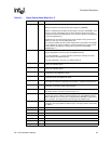
2.4 Memory Map
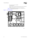
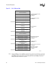
Figure 2-3 shows the SA-1110 memory map. The map is divided into four main partitions of
1 Gbyte each.
• Physical address: 0h0000 0000 to 0h3FFF FFFF.
This partition is dedicated to static memory devices (ROM, SRAM, and Flash) and to the
PCMCIA expansion bus area. This space is divided into:
— Four 128 Mbyte blocks for static memory devices
The static memory space is intended for ROM, SRAM, and Flash memory. The bottom
partition (at 0h0000 0000) is assumed to be ROM at boot time. The SMROM_EN pin is
used to determine if the boot ROM is asynchronous or synchronous. If asynchronous,
boot ROM is selected (SMROM_EN = 0), its width (16-bit or 32-bit) is determined by the
state of the ROM_SEL pin. SMROM is supported only on 32-bit data busses.
Note: The upper 64MBytes of each 128MByte static bank select cannot be accessed
because only 26 bits of the physical address are available on external pins. Attempts to
accesses any static bank selects upper 64Mbyte will actually cause an access to that bank
selects lower 64MByte, because the missing (27th) physical address bit is ignored.
— Two 256 Mbyte blocks for the PCMCIA interface
The PCMCIA interface is divided into Socket 0 and Socket 1 space. These partitions are
further subdivided into I/O, memory and attribute space.
• Physical address: 0h4000 0000 to 0h7FFF FFFF
This partition includes:
— Two 128 Mbyte blocks for static memory or variable latency I/O devices. This block
differs from the other three status memory spaces because it can be used for variable
latency I/O but not SRAM.
Note: The upper 64MBytes of each 128MByte static bank select cannot be accessed
because only 26 bits of the physical address are available on external pins. Attempts to
accesses any static bank selects upper 64Mbyte will actually cause an access to that bank
selects lower 64MByte, because the missing (27th) physical address bit is ignored.
— One 768 Mbyte block of reserved space. Accessing this reserved space results in a data
abort exception.
• Physical address: 0h8000 0000 to 0hBFFF FFFF
This partition contains all on-chip registers (except those specified by the ARM V4
architecture). This block is further divided into four 256 Mbyte blocks that contain control
registers for the following major functional blocks within the processor:
— Peripheral Control Module Registers
— System Control Module Registers
— Memory and Expansion Registers
— LCD and DMA Registers
• Physical address: 0hC000 0000 to 0hFFFF FFFF
This partition contains DRAM memory and is divided into:
— Four banks of DRAM fixed at 128 Mbyte each. With multiple banks implemented, there
probably will be gaps in the map that should be mapped through the
memory-management unit.