


SA-1110 Developer’s Manual 139
Memory and PC-Card Control Module
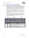
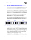
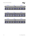
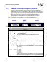
Table 10-4 describes how DRAM and synchronous memories can share MDCAS registers.
Key to Table: Tcpu – CPU clock period
trcd – RAS-to-CAS delay
tccd – CAS-to-CAS delay
tac – Delay from SDCLK rising edge to read data (D) latching edge
tcas – CAS low time
tcp – CAS high time
10.3.4 Static Memory Control Registers (MSC2 – 0)
MSC2, MSC1, and MSC0 are read/write registers and contain control bits for configuring static
memory (or variable latency I/O) that correspond to chip select pairs nCS[5:4], nCS[3:2], and
nCS[1:0], respectively. Timing fields are specified as numbers of memory clock cycles. The
memory clock cycle consists of two CPU cycles. Each of the three registers contains two identical
CNFG fields: one for each chip select within the pair. Please note the distinct descriptions for
nCS[5:3] variable latency I/O in the following MSCx register descriptions.
On hardware or sleep reset, the MSC0[15:0] field is set to 0b 1111 1111 1111 1x00 (binary) where
x represents the inverse of the ROM_SEL pin. This forces nCS(0) to the slowest possible nonburst
ROM timings. All other fields in MSC0, MSC1, and MSC2 are unaffected by reset. Question
marks indicate that the values are unknown at hardware or sleep reset.
Table 10-4. Timing Interpretations of Possible SDRAM/SMROM MDCAS Settings
Possible SDRAM/SMROM Settings for:
MDCASn0[31:0]
MDCASn1[31:0]
MDCASn2[31:0]
SDRAM/SMROM
Timing Interpretation
SDRAM LATCHING
KnDB2 = 0 KnDB2 = 1
delayed or
non-delayed
0101 0101 0101 0101 0101 0101 0101 0111
0101 0101 0101 0101 0101 0101 0101 0101
0101 0101 0101 0101 0101 0101 0101 0101
trcd=4*Tcpu
tccd=2*Tcpu
tac=2*Tcpu
trcd=4*Tcpu
tccd=4*Tcpu
tac=4*Tcpu
non-delayed read
1010 1010 1010 1010 1010 1010 1010 0111
1010 1010 1010 1010 1010 1010 1010 1010
1010 1010 1010 1010 1010 1010 1010 1010
trcd=4*Tcpu
tccd=2*Tcpu
tac=3*Tcpu
trcd=4*Tcpu
tccd=4*Tcpu
tac=4*Tcpu
delayed read
0101 0101 0101 0101 0101 0101 0101 1111
0101 0101 0101 0101 0101 0101 0101 0101
0101 0101 0101 0101 0101 0101 0101 0101
trcd=6*Tcpu
tccd=2*Tcpu
tac=2*Tcpu
Not Applicable non-delayed
read
1010 1010 1010 1010 1010 1010 1001 1111
1010 1010 1010 1010 1010 1010 1010 1010
1010 1010 1010 1010 1010 1010 1010 1010
trcd=6*Tcpu
tccd=2*Tcpu
tac=3*Tcpu
Not Applicable delayed read
0101 0101 0101 0101 0101 0101 0111 1111
0101 0101 0101 0101 0101 0101 0101 0101
0101 0101 0101 0101 0101 0101 0101 0101
trcd=8*Tcpu
tccd=2*Tcpu
tac=2*Tcpu
trcd=8*Tcpu
tccd=4*Tcpu
tac=4*Tcpu
non-delayed read
1010 1010 1010 1010 1010 1010 0111 1111
1010 1010 1010 1010 1010 1010 1010 1010
1010 1010 1010 1010 1010 1010 1010 1010
trcd=8*Tcpu
tccd=2*Tcpu
tac=3*Tcpu
trcd=8*Tcpu
tccd=4*Tcpu
tac=4*Tcpu
delayed read