


SA-1110 Developer’s Manual 185
Memory and PC-Card Control Module
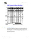
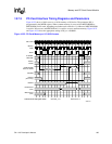
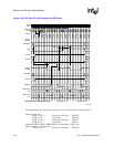
2*(BS_xx+1) second byte FAST=0
1*(BS_xx+1) + 1 half-word or first byte FAST=1
1*(BS_xx+1) second byte FAST=1
Address hold after command deassertion: BS_xx+1
nPWAIT valid after command assertion (max): 2*(BS_xx+1) - 2
Chip enable (nPCE1,2) setup to nPOE, nPWE assert:
3*(BS_xx+1) + 1 FAST=0
1*(BS_xx+1) + 1 FAST=1
Chip enable (nPCE1,2) setup to nPIOR, nPIOW assert:
3*(BS_xx+1) + 1 - (nIOIS16 delay from address) half-word or first byte FAST=0
2*(BS_xx+1) - (nIOIS16 delay from address) second byte FAST=0
1*(BS_xx+1) + 1 - (nIOIS16 delay from address) half-word or first byte FAST=1
1*(BS_xx+1) - (nIOIS16 delay from address) second byte FAST=1
Chip enabled hold from command deassert: BS_xx+1
See Chapter 13, “AC Parameters” for actual AC timing.
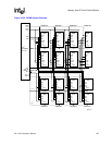
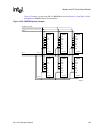
10.8 Alternate Memory Bus Master Mode
The SA-1110 supports the existence of an alternate master on the DRAM memory bus. The
alternate master is given control of the bus using a hardware handshake. This handshake is
performed through MBREQ and MBGNT, which are invoked through the alternate functions on
GPIO 22 and GPIO 21, respectively. When the alternate master wants to take control of the
memory bus, it asserts MBREQ (GPIO 22). The SA-1110 will complete any pending or in-progress
memory operation and any outstanding DRAM refresh cycle. It then deasserts SDCKE 1 and
tristates all memory bus pins used with DRAM bank 0 (nRAS/nSDCS 0, A[25:0], nOE, nWE,
nSDRAS, nSDCAS, SDCLK 1, D[31:0], nCAS/DQM[3:0]). All other memory and PC-Card pins
remain driven, including SDCLK 2 is driven to 0, SDCLK 0 is driven to 0, and SDCKE 0 is driven
to 1. The RD/nWR pin will remain low. Then the SA-1110 will assert MBGNT (GPIO 21), the
alternate master should start driving all pins (including SDCLK 1), and the SA-1110 will re-assert
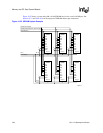
SDCKE 1. The grant sequence and timing are as follows; the Tmem unit of time is the memory
clock period (twice the CPU clock period):
— Alternate master asserts MBREQ
— SA-1110 deasserts SDCKE 1 at time (t)
— SA-1110 begins to tristate DRAM outputs at time (t + 1*Tmem)
— SA-1110 asserts MBGNT at time (t + 2*Tmem)
— Alternate master begins to drive DRAM outputs prior to time (t + 3*Tmem)
— SA-1110 asserts SDCKE 1 at time (t + 4*Tmem)
During the tristate period, both MBREQ and MBGNT remain high and an external device may take
control of the tristated pins. The external device should drive all the tristated pins even if some are
not actually used. Otherwise, floating inputs may cause excessive crossover current and/or
erroneous SDRAM commands. Note that during the tristate period, the SA-1110 is unable to
perform DRAM refresh cycles. The alternate master must assume the responsibility for DRAM
integrity during this period. It is recommended that the system be designed such that the period of
alternate mastership is limited to much less than the refresh period, or that the alternate master
implement a refresh counter making it capable of performing refresh at the proper intervals.