SA-1110 Developer’s Manual 151
Memory and PC-Card Control Module
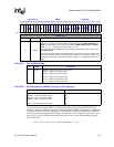
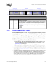
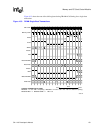
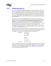
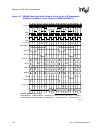
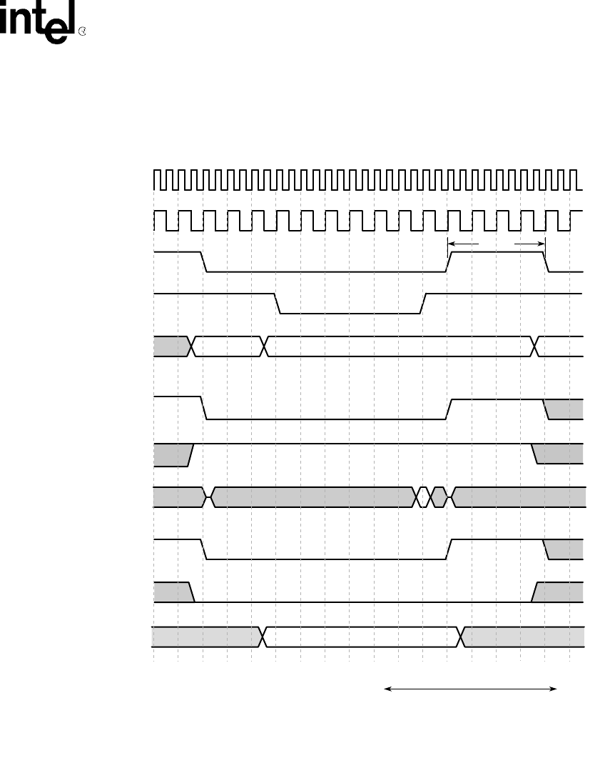
Figure 10-3 shows the rate of the shift registers during DRAM nCAS timing for a single-beat
transaction.
Figure 10-3. DRAM Single-Beat Transactions
A6633-02
CPU Clock
Memory Clock
ADDR
Reads:
nOE
TRP+1
nRAS
nCAS
Read RD/nWR
COL
D0
ROWROW
Writes:
Read Data
Write RD/nWR
Contents of DRAM register fields:
MDCAS0
1 =
11 0001 1000 1100
(binary)
MDCAS0
0 =
0110 0011 0001 1000 1100 0110 0000 0111
(binary)
MDCNFG:TRP0 = 4 MDCNFG:CDB20 = 1 TDL0 = 00
nWE
firstlast
time
Write Data
DO


