


132 SA-1110 Developer’s Manual
Memory and PC-Card Control Module
10.3.2 DRAM Refresh Control Register (MDREFR)
MDREFR is a read/write register and contains control bits for refresh of both DRAM bank pairs.
The DRAM refresh interval field applies to all types of DRAM (asynchronous and synchronous).
MDREFR also contains control/status bits for SDRAM self-refresh, SDRAM/SMROM clock
divisors, SDRAM/SMROM clocks running, and SDRAM/SMROM clock enable pin states.
Independent control/status is provided for each of the clock pins (SDCLK[2:0]) and clock enable
pins (SDCKE [1:0]). Question marks indicate that the values are unknown at hardware or sleep
reset. Writes to reserved bits are ignored and reads return zeros.
The clock run bits (K0RUN, K1RUN, and K2RUN) and clock enable bits (E0PIN and E1PIN)
provide ultimate software control of SDRAM and SMROM low power modes. They should be
used with extreme caution; when any of these bits are cleared, the corresponding memory is
inaccessible. Upon hardware or sleep reset, K0RUN and E0PIN are set to the value of the
SMROM_EN pin.
Auto-power-down, enabled by the KAPD and EAPD bits, is an automatic mechanism for
minimizing power consumption in the SA-1110 SDCLK pin drivers and the SDRAM/SMROM
devices. EAPD and KAPD must be written to the same value. A latency penalty of one memory
cycle (two CPU cycles) is incurred when re-starting SDCLK and/or SDCKE between
non-consecutive SDRAM/SMROM transfers.
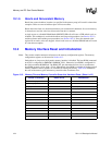
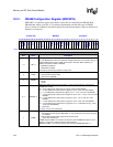
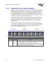
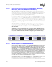
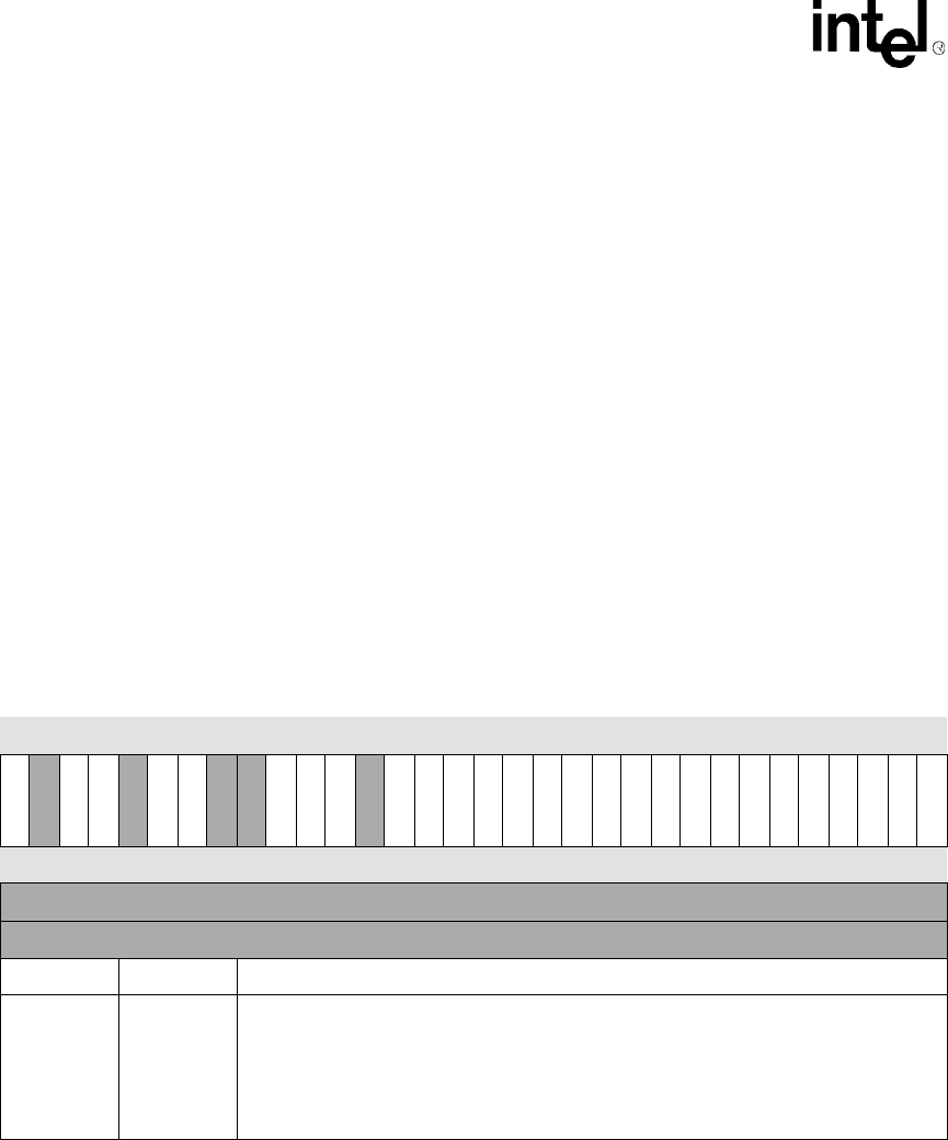
0h A000 001C MDREFR Read/Write
31 30 29 28 27 26 25 24 23 22 21 20 19 18 17 16 15 14 13 12 11 10 9 8 7 6 5 4 3 2 1 0
SLFRSH
Reserved
KAPD
EAPD
Reserved
K2DB2
K2RUN
Reserved
Reserved
K1DB2
K1RUN
E1PIN
Reserved
K0DB2
K0RUN
E0PIN
DRI11
DRI10
DRI9
DRI8
DRI7
DRI6
DRI5
DRI4
DRI3
DRI2
DRI1
DRI0
TRASR3
TRASR2
TRASR1
TRASR0
Reset 1 ? 0 0 ? 1 0 ? ? 1 0 0 ? 1 * * ? ? ? ? ? ? ? ? ? ? ? ? ? ? ? ?
* Upon hardware or sleep reset, K0RUN and E0PIN are set to the value of the SMROM_EN pin.
(Sheet 1 of 4)
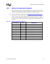
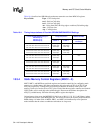
Bits Name Description
3..0 TRASR 3..0
RAS assertion during CBR, all banks.
For asynchronous DRAM, TRASR is encoded with the number of memory clocks (minus
one) that nRAS/nSDCS is asserted during CAS before RAS refresh.
For systems with SDRAM, TRASR must be at least one (1) to cause the required one clock
assertion of nRAS/nSDCS and nCAS/DQM. If a system contains no asynchronous DRAM,
TRASR=1 should be used to minimize the CBR duration.