


SA-1110 Developer’s Manual 375
Peripheral Control Module
11.12.10.3 Loopback Mode (LBM)
The loopback mode (LBM) bit is used to enable and disable the ability of the SSP transmit and
receive logic to communicate. When LBM=0, the SSP operates normally. The transmit and receive
data paths are independent and communicate via their respective pins. When LBM=1, the output of
the transmit serial shifter is directly connected to the input of the receive serial shifter internally
and control of the TXD4, RXD4, SCLK, and SFRM pins are given to the peripheral pin control
(PPC) unit.
11.12.10.4 Serial Clock Polarity (SPO)
The serial clock polarity (SPO) bit selects the polarity or active/inactive state of the serial clock
(SCLK) pin when Motorola SPI format is selected (FRF=00). When SPO=0, the inactive or idle
state of SCLK is low. Thus when the SSP is not actively transmitting/receiving data, the SCLK pin
is held low. When SPO=1, the inactive or idle state of SCLK is high. Thus when the SSP is not
actively transmitting/receiving data, the SCLK pin is held high. The programming of SPO alone
does not determine which SCLK edges are used to drive and latch data to or from the transmit and
receive pins. The programming of SPO and the serial clock phase (SPH) bit determines this. Note
that SPO is ignored in all other modes except Motorola SPI format (FRF=00).
11.12.10.5 Serial Clock Phase (SPH)
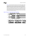
The serial clock phase (SPH) bit selects the phase relationship of the serial clock (SCLK) signal
with the serial frame (SFRM) signal when Motorola SPI format is selected (FRF=00). When
SPH=0, SCLK remains in its inactive state (as programmed by SPO) for one full SCLK period
duration after SFRM is asserted (driven low). SCLK continues to transition during the entire frame
and is driven to its inactive state one-half SCLK period duration before SFRM is negated (driven
high). When SPH=1, SCLK remains in its inactive state (as programmed by SPO) for one-half
SCLK period duration after SFRM is asserted (driven low). SCLK continues to transition during
the entire frame and is driven to its inactive state one full SCLK period duration before SFRM is
negated (driven high). Using SPH and SPO together determine when SCLK is active during the
assertion of SFRM and which edge of SCLK is used to drive data to the transmit pin as well as
latch data from the receive pin. When SPO and SPH are the same value (both 0 or both 1), transmit
data is driven on the falling edge of SCLK and receive data is latched on the rising edge of SCLK.
Alternatively, when SPO and SPH are of opposite value (one 0 and the other 1), transmit data is
driven on the rising edge of SCLK and receive data is latched on the falling edge of SCLK. Note
that SPH is ignored in all other modes, except Motorola SPI format (FRF=00).
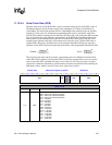
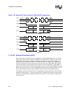
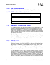
Figure 11-36 shows the pin timing for all four programming combinations of SPO and SPH. Note
that SPO inverts the polarity of the SCLK signal, and SPH determines the phase relationship
between SCLK and SFRM, shifting the SCLK signal one-half phase to the left or right during the
assertion of SFRM.