


SA-1110 Developer’s Manual 401
AC Parameters
13.6 Timing Parameters
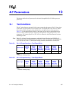
Table 13-3 lists AC timings for SDRAM and SMROM. It includes frequency-dependent guidelines
for using the delayed latching option on read data. This option is controlled by the contents of the
CAS Waveform Rotate Registers (MDCASnn), as described in Section 10.3.3.2, “MDCAS
Registers with SDRAM and SMROM” on page 10-137.
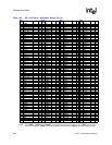
Table 13-4 lists the AC timing guidelines for asynchronous memory types. Each parameter
references the SA-1110’s internal memory clock. These parameters are not guaranteed for use
under all operating conditions.
Table 13-5 lists the AC timing parameters for the SA-1110 MCP interface and LCD controller. For
timing parameters for 1.55-V devices, contact the Intel Massachusetts Customer Technology
Center.
NOTES:
1. Tsdis and Tsdih are specified for non-delayed read data latching on 133 MHz (AC, AD) and 206 MHz (BC,
BD) devices, and for delayed read data latching at the maximum SDCLK frequency on AC and AD devices
(103 MHz when using a 3.6864 MHz crystal). All other Tsdis and Tsdih values (i.e.- those for delayed read
data latching on BC and BD devices with SDCLK between 62 MHz and 98 MHz) should be considered as
guidelines, and are not guaranteed for use under all operating conditions.
2. The larger Tsdih values can be achieved by intentionally adding delay to SDCLK (e.g., by using serpentine
board routing). However, the system designer must carefully evaluate the resulting degradation to input setup
time and output hold time: Tsdis and Tsdoh increase and decrease, respectively, from the corresponding
table values.
3. When SDRAM/SMROM is configured to run at one-half the memory clock frequency (e.g., MDREFR:K0DB2
= 1 for SMROM), the minimum output setup time is increased from Tsdos by approximately one memory
clock period. This helps to accommodate SMROM, which typically requires both a lower frequency and larger
setup times than SDRAM.
4. Tsdos (output setup time) is specified for comparison to memory specifications' input setup time parameters.
Tsdos is specifying the minimum time the signal will be valid before the SDCLK[2:0] rising edge.
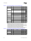
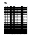
Table 13-3. SA-1110 AC Timing Specifications and Guidelines for SDRAM/SMROM
Pin Name Symbol Parameter
AC, AD (133
MHz max)
BC, BD (206
MHz max)
SDCLK
Frequency
(MHz)
Non-Delayed
or Delayed
Latching on
Read Data
Min Unit Note
Memory Bus
A[25:0[, D[31:0],
nRAS/nSDCS[3:0],
nCAS/DQM[3:0], nCS[3:0],
nSDRAS, nSDCAS, nWE, nOE,
SDCKE[1:0]
Tsd os
SDRAM/ SMROM
output setup time to
SDCLK[2:0] rise
AC 28 - 66 2.2 ns 3,4
BC 28 - 103 2.2 ns 3,4
A[25:0], D[31:0],
nRAS/nSDCS[3:0],
nCAS/DQM[3:0], nCS[3:0],
nSDRAS, nSDCAS, nWE, nOE,
SDCKE[1:0]
Tsd oh
SDRAM/ SMROM
output hold time
from SDCLK[2:0]
rise
AC 28 - 66 2.2 ns
BC 28 - 103 2.2 ns
D[31:0]
Tsd is
SDRAM/ SMROM
data input setup
time to SDCLK[2:0]
rise
AC 28 - 66 Non-Delayed 7.2 ns 1
BC
28 - 62 Non-Delayed 9.3 ns 1
62 - 103 Delayed 2.7 ns 1
D[31:0]
Tsd ih
SDRAM/ SMROM
data input hold time
from SDCLK[2:0]
rise
AC 28 - 66 Non-Delayed 2.7 ns 1
BC
28 - 62 Non-Delayed 2.7 ns 1
62 - 69 Delayed 5.5 ns 1, 2
69 - 76 Delayed 4.7 ns 1, 2
76 - 84 Delayed 4.1 ns 1, 2
84 - 91 Delayed 3.6 ns 1, 2
91 - 98 Delayed 3.1 ns 1, 2
98 - 103 Delayed 2.7 ns 1