


SA-1110 Developer’s Manual 137
Memory and PC-Card Control Module
of 2 CPU clock cycles). When MDCNFG:CDB20 is "1" or MDCNFG:DWID0 is "1", the
MDCAS00 must contain "1"s in the lower 2 bits and each transition of nCAS/DQM must be a
minimum of 1 bit.
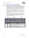
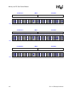
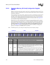
10.3.3.2 MDCAS Registers with SDRAM and SMROM
See Table 10-4 “Timing Interpretations of Possible SDRAM/SMROM MDCAS Settings” on
page 10-139 for a description of possible MDCAS encodings for SDRAM or SMROM. nSDCAS
asserts as indicated by the first "1" to "0" transition: similar to the behavior of nCAS/DQM for
asynchronous DRAM. But, because the least significant bit of MDCAS goes out on nSDCAS one
CPU cycle after the assertion of nRAS/nSDCS, the RAS-to-CAS delay is one CPU cycle greater
than the number of leading 1's. Thus, a RAS-to-CAS delay of N memory cycles (2N CPU cycles)
corresponds to 2N-1 leading 1's. When using MDREFR: KnDB2=0 (SDCLK = memory clock), the
number of leading 1's must be 3, 5, 7, ... to achieve a RAS-to-CAS delay of 2, 3, 4, ... SDCLK
cycles.
EXAMPLE: RAS-to-CAS delay of 2 SDCLK cycles:
When KnDB2 = 0, 1 SDCLK cycle = 1 memory clock cycle = 2 CPU clock cycles
RAS-to-CAS delay of 2 SDCLK cycles = 2 memory cycles = 4 CPU cycles
Number of required leading zeros = 4 - 1 (for nRAS to MDCAS delay) = 3
When using MDREFR: KnDB2=1 (SDCLK = 1/2 memory clock), the number of leading 1's must
be 3, 7, 11, ... to achieve a RAS-to-CAS delay of 1, 2, 3, ... SDCLK cycles.
EXAMPLE: RAS-to-CAS delay of 3 SDCLK cycles:
When KnDB2 = 1, 1 SDCLK cycle = 2 memory clock cycles = 4 CPU cycles
RAS-to-CAS delay of 3 SDCLK cycles = 6 memory cycles = 12 CPU cycles
Number of required leading zeros = 12 - 1 (for nRAS to MDCAS delay) = 11
For SDRAM, nSDCAS remains asserted throughout the burst, regardless of subsequent transitions
programmed into MDCAS. For SMROM, nSDCAS is asserted only through the first column
address. In either case, subsequent "0" to "1" transitions must be programmed to reference the data
input latch delay (MDCNFG:TDL0,2 or SMCNFG:CL0,2) for every beat of the burst. There must
be either one or two "0" bits between the leading 1's for RAS-to-CAS delay and the next "1". The
option of using one such "0" bit is referred to as "non-delayed read data latching" in the Table 13-3
SDRAM/SMROM timing specifications and guidelines. The option of using two such "0" bits,
referred to as "delayed read data latching", provides an additional half memory cycle of read data
setup time. The latter option is ignored unless MDREFR:KnDB2=0, and is useful under the
following common circumstances (evaluated for specific load):
Note: Subsequent to the first "0" to "1" transition, MDCAS must be filled through the 96th bit with the
2-bit repeating pattern of "0" followed by "1".
Chapter 13, “AC Parameters” provides frequency-dependent guidelines for using the delayed
latching option.
max(mem clock to SDCLK delay) + max(SDCLK to data delay) + max(data to mem clock set up) >= Tmem
max(mem clock to SDCLK delay) + max(SDCLK to data delay) + max(data to mem clock set up) <= Tmem + Tcpu
min(mem clock to SDCLK delay) + min(SDCLK to data delay) + min(data to mem clock set up) >= Tcpu