


328 SA-1110 Developer’s Manual
Peripheral Control Module
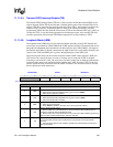
use of the sample clock input, and loopback mode. The data register is 8 bits and addresses the top
location of the transmit FIFO and bottom location of the receive FIFO. When it is read, the receive
FIFO is accessed, and when it is written, the transmit FIFO is accessed. The status registers contain
bits that signal the transmit FIFO service request, receive FIFO service request, receiver idle, the
begin and end of break detect, and error in FIFO conditions. Each of these status conditions signal
an interrupt request to the interrupt controller. The status registers also flag when the UART is
actively transmitting characters, when the transmit FIFO is not full, when the receive FIFO is not
empty, and when a parity, framing, or overrun error was detected for the data value currently
located in the bottom entry of the receive FIFO (no interrupt generated).
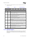
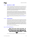
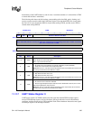
11.11.3 UART Control Register 0
UART control register 0 (UTCR0) contains seven different bit fields that control various functions
within the UART.
11.11.3.1 Parity Enable (PE)
The parity enable (PE) bit is used to enable or disable parity checking by the receive data logic as
well as parity generation by the transmit logic. When parity is enabled (PE=1), the odd/even parity
select (OES) control bit is decoded to determine which type of parity should be checked and
generated. The parity of each data frame received is checked. If the parity type programmed in the
OES bit does not match the parity of the data received, the parity error (PRE) bit is set in the same
entry in the receive FIFO where the errant data resides. When parity is disabled (PE=0), the parity
check and generation logic is disabled, parity bits are not inserted into transmitted frames, and the
receive logic expects a stop bit to occur after the MSB of each data value is received.
11.11.3.2 Odd/Even Parity Select (OES)
The odd/even parity select (OES) bit is used to select whether odd or even parity should be used by
the transmit and receive logic. When OES=0, odd parity is selected; when OES=1, even parity is
selected. When parity is enabled (PE=1), the parity bit is placed after the data’s MSB in each frame.
The transmit logic sets or clears the parity bit to make the total number of ones transmitted
(including the parity bit) match the parity type programmed using OES
(if even parity is selected (OES=1) and there is an odd number of ones in the data to be
transmitted, the parity bit is set). The receive data logic counts the number of ones encountered in
the incoming data stream (including the parity bit), then strips the parity bit from the data. If the
parity type of the frame does not match the parity selected by OES, the parity error bit is set (bit 8)
within the FIFO entry corresponding to the data that produced the parity error.
11.11.3.3 Stop Bit Select (SBS)
The stop bit select (SBS) bit selects whether one or two stop bits should be used in transmission.
When SBS=0, one stop bit is inserted in the transmit frame for each character. When SBS=1, two
stop bits are inserted. SBS does not affect the UART’s receive logic. The receiver always checks to
make sure there is at least one stop bit per character.