


314 SA-1110 Developer’s Manual
Peripheral Control Module
stored in the receive FIFO. The address value is contained within the first byte of data in a frame
following the flag. AMV can be written at any time and is used for comparison with the next frame,
which occurs following its update.
Note: A question mark (?) signifies that the Reset value of that bit is undefined when the processor has
completed its reset cycle.
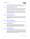
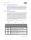
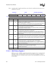
The following table shows the address match value field within HSSP control register 1. The reset
state of AMV is unknown (indicated by question marks) and must be initialized before enabling the
HSSP. Note that HSCR1 may be written while the HSSP is enabled to allow the address match
value to be changed during active receive operation.
11.10.8 HSSP Control Register 2
The HSSP control register 2 (HSCR2) contains two bit-fields that control the polarity of the
transmit and receive data pins. Note that unlike the rest of the HSSP’s registers, its bits are located
in byte 2 of the addressed word (bits 23..16). Word reads or writes should be used to access this
register. Also note that this register resides within the PPC’s address space.
11.10.8.1 Transmit Pin Polarity Select (TXP)
The transmit pin polarity select (TXP) bit is used to select whether data output to the ICP’s transmit
pin (TXD2) is true or complemented. When TXP=0, data output from the UART (low-speed
mode), HSSP (high-speed mode), or PPC (GPIO output mode) is inverted first before being output
to the TXD2 pin. When TXP=1, data output from either the UART, HSSP, or PPC to the TXD2 pin
is true or noninverted. TXP is initialized to 1 following reset such that output pin data defaults to
true data.
Note that TXP affects the TXD2 pin during all modes of operation including HSSP, UART, and
PCC. The user should ensure that this bit is properly programmed when using serial port 2 for high-
or low-speed IrDA, normal UART, or GPIO operation. Note that for GPIO mode, the user needs to
configure TXP only when the pin is to be used as an output (PPDR 14=1). When used as a GPIO
input, TXP has no effect on the state of TXD2. See the Peripheral Pin Controller chapter.
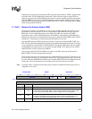
0h 8004 0064 HSCR1 Read/Write
7 6 5 4 3 2 1 0
AMV
Reset
? ? ? ? ? ? ? ?
Bits Name Description
7..0 AMV
Address match value.
The 8-bit value used by receiver logic to compare to address of incoming frames. If AME=1
and AVM matches the address of the incoming frame, store the frame address, control,
and data in receive FIFO; if address does not match, ignore the frame and search for the
next preamble.
Note: An address of 0hFF (all ones) in the incoming frame automatically generates a
match (AMV is ignored).