


186 SA-1110 Developer’s Manual
Memory and PC-Card Control Module
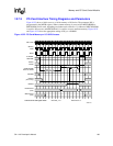
To relinquish the bus, the alternate master deasserts MBREQ. The SA-1110 deasserts SDCKE 1
and deasserts MBGNT, the alternate master stops driving all the DRAM pins (including SDCLK
1), the SA-1110 resumes driving all DRAM pins (including SDCLK 1), and the SA-1110 re-asserts
SDCKE 1. The release sequence and timing are as follows:
— Alternate master deasserts MBREQ
— SA-1110 deasserts SDCKE 1 at time (t)
— SA-1110 deasserts MBGNT at time (t + 1*Tmem)
— Alternate master tristates DRAM outputs prior to time (t + 2*Tmem)
— SA-1110 begins to drive DRAM outputs at time (t + 3*Tmem)
— SA-1110 asserts SDCKE 1 at time (t + 4*Tmem)
If the refresh counter inside the SA-1110 requested a refresh cycle during the alternate master
tenure, then that refresh cycle is run first, followed by any other bus transactions that stalled during
that period.
This mode is set up by writing registers as follows:
• Write the GPIO pin direction register (GPDR) at physical address 0x9004 0004 to set bit 21
(make GPIO 21 an output) and clear bit 22 (make GPIO 22 an input).
• Write the GPIO alternate function register (GAFR) at physical address 0x9004 001C to set bits
21 (enable the MBGNT alternate output function) and 22 (enable the MBREQ alternate input
function).
• Write the test unit control register (TUCR) at physical address 0x9003 0008 to set bit 10
(enable the memory request mode).
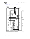
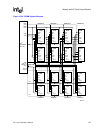
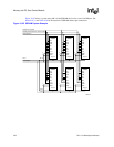
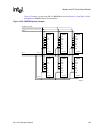
10.9 Memory System Examples
This section gives examples of memory systems that are possible with the SA-1110. Figure 10-24
shows a system using 1M x 16 DRAMs for a total of 16 Mbytes of DRAM. Two banks of ROM
and two banks of Flash memory are shown. Each on a 32-bit wide data bus. The PC-Card interface
is not shown.