


SA-1110 Developer’s Manual 127
Memory and PC-Card Control Module
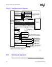
10.3 Memory Configuration Registers
The SA-1110 memory interface is programmed through a set of configuration registers that are
described in the following sections. Many timing parameters are encoded as a number of memory
clock cycles, where each memory clock cycle is equivalent to two CPU clock cycles.
Note: There is an online memory configuration tool at http://appzone.intel.com/hcd/sa1110/memory
which can be used to help configure the SA-1110 for operation with the user’s choice of memory.
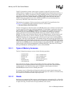
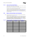
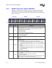
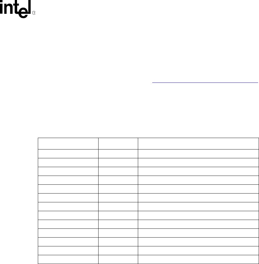
Table 10-3 shows the registers associated with the memory interface and the physical addresses
used to access them. All addressing is little endian. These registers are readable and writable only
as full words. They are grouped together within one page and thus all have the same memory
protections.
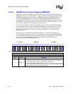
Table 10-3. Memory Interface Control Registers
Physical Address Symbol Register Name
0xA000 0000 MDCNFG DRAM configuration register
0xA000 0004 MDCAS00 CAS waveform rotate register 0 for DRAM bank pair 0/1
0xA000 0008 MDCAS01 CAS waveform rotate register 1 for DRAM bank pair 0/1
0xA000 000C MDCAS02 CAS waveform rotate register 2 for DRAM bank pair 0/1
0xA000 0010 MSC0 Static memory control register 0
0xA000 0014 MSC1 Static memory control register 1
0xA000 0018 MECR Expansion memory (PC-Card) bus configuration register
0xA000 001C MDREFR DRAM refresh control register
0xA000 0020 MDCAS20 CAS waveform rotate register 0 for DRAM bank pair 2/3
0xA000 0024 MDCAS21 CAS waveform rotate register 1 for DRAM bank pair 2/3
0xA000 0028 MDCAS22 CAS waveform rotate register 2 for DRAM bank pair 2/3
0xA000 002C MSC2 Static memory control register 2
0xA000 0030 SMCNFG SMROM configuration register