


SA-1110 Developer’s Manual 163
Memory and PC-Card Control Module
10.6.1 ROM Interface Overview
The SA-1110 provides programmable timing for both burst and non-burst ROMs. The RDF field in
MSCx is the latency (in memory clock cycles) for the first and all subsequent data beats from
nonburst ROMs, and the first data beat from a burst ROM. RDN is the latency for the burst data
beats after the first for burst ROMs. RRR delays the following access to a different memory space
to allow time for the current ROM to tristate the data bus. This parameter should be programmed
with the maximum t
OFF
value, as specified by the ROM manufacturer. One memory clock cycle is
always added to RDF and RDN. One memory clock cycle is added to RRR if it was set to zero,
otherwise RRR is doubled. Upon hardware or sleep reset, MSC0[15:0] is initialized such that the
RDF, RDN and RRR fields are set to their maximum values to accommodate the slowest nonburst
ROMs at initial boot, RT is set to be nonburst ROM, and RBW0 is loaded with the value of the
inverse of the ROM_SEL pin. The remaining fields in MSC0, MSC1, and MSC2 are not initialized
on hardware or sleep reset. MSC0[15:0] is selected when the address space corresponding to nCS0
is accessed.
The SA-1110 supports a ROM burst size of 1, 4 or 8. A single CBR refresh cycle, for asynchronous
DRAM and/or SDRAM, may be inserted between word accesses within a burst transaction. nCS
and nOE are deasserted during the refresh cycle.
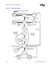
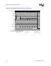
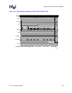
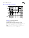
10.6.2 ROM Timing Diagrams and Parameters
Figure 10-10, Figure 10-11,andFigure 10-12 show the timing for burst and nonburst ROMS.
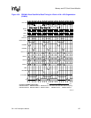
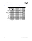
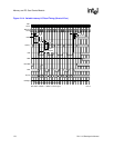
01
Variable
Latency I/O
nCS[5:3]
Reads,
Writes
Reads,
Writes
RDF+
RDN+2+
waits
RDF+1+
waits
RDN+1
RDF+
RDN+2+
waits
RDF+1+
waits
RDN+1
10
Burst-of-4
ROM or
Flash
(nonburst
writes)
nCS[5:0]
Reads,
Writes
Reads
RDF+1
[0,4]
RDN+1
[1:3],
[5:7]
RDF+1
[0,4]
RDN+1
[1:3],
[5:7]
0 N/A RDF+1 N/A
11
Burst-of-8
ROM or
Flash
(nonburst
writes)
nCS[5:0]
Reads,
Writes
Reads
RDF+1
(0)
RDN+1
[1:7]
RDF+1
(0)
RDN+1
[1:7]
0 N/A RDF+1 N/A
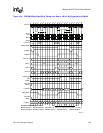
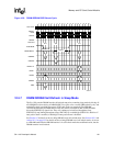
Table 10-10. Summary of Static Memory and Variable Latency I/O Capabilities
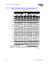
MSCx:
RT
Device
Type
Chip
Selects
Directions
Supported
for Single
Internal
Transfers
Directions
Supported
for Burst
Internal
Transfers
Timing (Memory Clocks)
Burst
Read
Address
Assert
nOE
Assert
Burst
nOE
De-
assert
Burst
Write
Address
Assert
nWE
Assert
Burst
nWE
De-
assert