


144 SA-1110 Developer’s Manual
Memory and PC-Card Control Module
10.4 SMROM Configuration Register (SMCNFG)
SMCNFG is a read/write register and contains control bits for configuring SMROM. Both
SMROM banks within a pair (nCS[1:0] or nCS[3:2]) must be implemented with the same type of
device, but the two bank pairs may differ. Question marks indicate that the values are unknown at
hardware or sleep reset. Writes to reserved bits are ignored and reads return zeros.
If any of the nCS[3:0]) banks is configured for synchronous mask ROM (SMROM) via
SMCNFG:SM[3:0], the corresponding half-words of MSC0 and/or MSC1 are ignored.
Note: Upon hardware or sleep reset, SM0 is set to the value of the SMROM_EN pin.
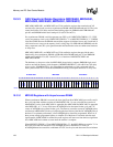
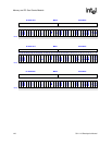
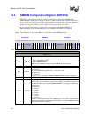
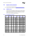
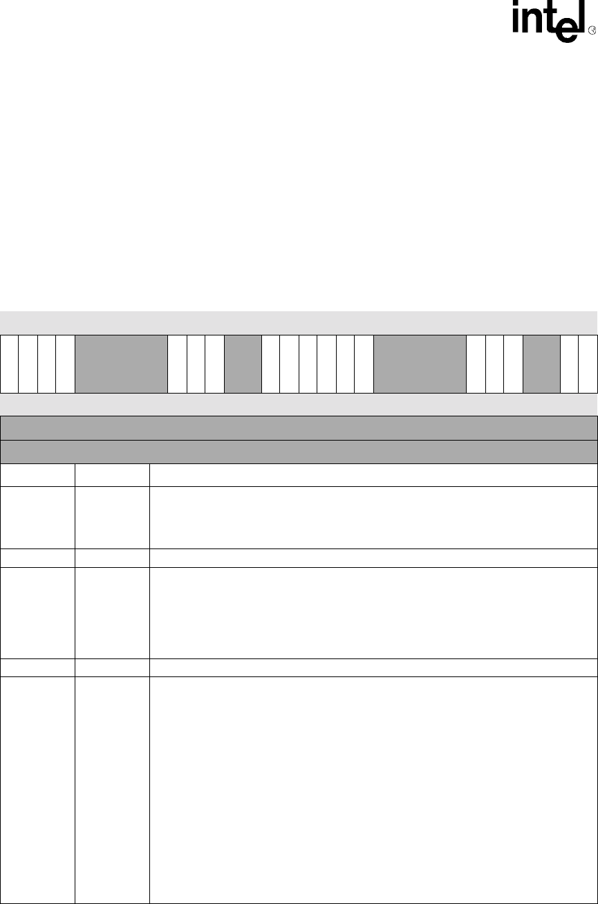
0h A000 0030 SMCNFG Read/Write
31 30 29 28 27 26 25 24 23 22 21 20 19 18 17 16 15 14 13 12 11 10 9 8 7 6 5 4 3 2 1 0
RL2
CL22
CL21
CL20
Reserved
RA22
RA21
RA20
Reserved
SM3
SM2
RL0
CL02
CL01
CL00
Reserved
RA02
RA01
RA00
Reserved
SM1
SM0
Reset ? ? ? ? ? ? ? ? ? ? ? ? ? ? 0 0 1 1 0 0 ? ? ? ? ? 1 0 0 ? ? 0 *
* Upon hardware or sleep reset, SM0 is set to the value of the SMROM_EN pin.
(Sheet 1 of 3)
Bits Name Description
1..0 SM 1..0
SMROM enables for bank 1 (bit 1) and bank 0 (bit 0).
0 - Bank is not SMROM enabled.
1 - Bank is SMROM enabled.
SM0 is set upon hardware or sleep reset if the SMROM_EN pin is held high.
3..2 — Reserved.
6..4 RA0 2..0
SMROM row address bit count for bank pair 0/1.
0xx - Reserved.
100 - 13 row address bits, supports 13x11, 13x10, 13x9, 13x8.
101 - Reserved.
11x - Reserved.
See Table 10-8 for a description of DRAM or SMROM row/column address multiplexing.
11..7 — Reserved.
14..12 CL0 2..0
CAS latency for bank pair 0/1.
It is the number of external SDCLK cycles between reception of the READ command and
latching of the data. The unit size for CL0 is the external SDCLK cycle: when SMROM is
run at half the memory clock frequency (MDREFR:K0DB2 = 1), the delay is 2*CL0 internal
memory cycles.
000 - Reserved.
001 - 2 clocks.
010 - 3 clocks.
011 - 4 clocks.
100 - 5 clocks.
101 - 6 clocks.
110 - 7 clocks.
111 - Reserved.
Hardware or sleep reset forces CL0=100. If SMROM_EN=1, CL0 must be maintained at this
value to avoid a mismatch in CAS latency between the SA-1110 and boot SMROM following
a subsequent hardware or sleep reset.