


128 SA-1110 Developer’s Manual
Memory and PC-Card Control Module
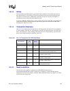
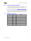
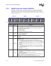
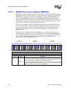
10.3.1 DRAM Configuration Register (MDCNFG)
MDCNFG is a read/write register and contains control bits for configuring the DRAM. Both
DRAM banks within a pair (0/1 or 2/3) must be implemented with the same type of DRAM
devices, but the two bank pairs may differ. Question marks indicate that the values are unknown at
hardware or sleep reset.
0h A000 0000 MDCNFG Read/Write
31 30 29 28 27 26 25 24 23 22 21 20 19 18 17 16 15 14 13 12 11 10 9 8 7 6 5 4 3 2 1 0
TWR21
TWR20
TDL21
TDL20
TRP23
TRP22
TRP21
TRP20
CDB22
DRAC22
DRAC21
DRAC20
DWID2
DTIM2
DE3
DE2
TWR01
TWR00
TDL01
TDL00
TRP03
TRP02
TRP01
TRP00
CDB20
DRAC02
DRAC01
DRAC00
DWID0
DTIM0
DE1
DE0
Reset ? ? ? ? ? ? ? ? ? ? ? ? ? ? 0 0 ? ? ? ? ? ? ? ? ? ? ? ? ? ? 0 0
(Sheet 1 of 4)
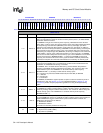
Bits Name Description
1..0 DE1..0
DRAM enable for bank 1 (bit 1) and bank 0 (bit 0).
For each DRAM bank, there is an enable bit. A single (nonburst) access (read or write) to a
disabled DRAM bank triggers a CBR refresh cycle to all banks. When all banks are
disabled, the refresh counter is disabled.
0 – DRAM bank disabled.
1 – DRAM bank enabled.
These bits are cleared by hardware or sleep reset.
2DTIM0
DRAM timing type for bank pair 0/1.
0 – Asynchronous (FPM or EDO).
1 – Synchronous (SDRAM).
3DWID0
DRAM data bus width for bank pair 0/1.
0 – 32 bits.
1 – 16 bits.
6..4 DRAC02..0
DRAM row address bit count for bank pair 0/1. This count includes one or two bits for
SDRAM bank selects.
000 – 9 row address bits. (Select this for support of 9x9 and 9x8 DRAMs.)
001 – 10 row address bits. (Select this for support of 10x10, 10x9, and 10x8 DRAMs.)
010 – 11 row address bits. (Select this for support of 11x11, 11x10, 11x9, and 11x8 DRAMs.)
011 – 12 row address bits. (Select this for support of 12x12, 12x11, 12x10, 12x9, and 12x8
DRAMs.)
100 – 13 row address bits. (Select this for support of 13x11, 13x10, 13x9, and 13x8
DRAMs.)
101 – 14 row address bits. (Select this for support of 14x10, 14x9, and 14x8 DRAMs.)
110 – 15 row address bits. (Select this for support of 15x11 (16-bit data bus only), 15x10,
15x9, and 15x8 DRAMs.)
111 – Reserved.
See Table 10-8 for more information.
7 CDB20
Clock divide by 2 for bank pair 0/1.
0 – CAS waveform rotate register (MDCAS00, 01, 02) rotated every CPU clock. Required
for SDRAM.
1 – CAS waveform rotate register rotated every memory clock.
(CPU clock divided by 2.)
SDRAM requires CDB20 = 0. However, the frequency of the SDRAM bank pair 0/1 clock
(SDCLK 1) can be set to either the memory clock frequency
(MDREFR:K1DB2 = 0) or half the memory clock frequency (MDREFR:K1DB2 = 1).