


334 SA-1110 Developer’s Manual
Peripheral Control Module
11.11.6 UART Data Register
The UART data register (UTDR) is an 8-bit register corresponding to both the top and bottom
entries of the transmit and receive FIFOs, respectively.
When UTDR is read, the lower 8 bits of the bottom entry of the 10-bit receive FIFO are accessed. As
data enters the top of the receive FIFO, bits 8..10 are used to indicate various error conditions that
occur during reception of each piece of data. The error bits are transferred down the FIFO along with
the value that caused the error. When data reaches the bottom, bit 8 of the bottom FIFO entry is
automatically transferred to the parity error (PRE) flag, bit 9 to the framing error (FRE) flag, and bit
10 to the receiver overrun (ROR) flag, all within the UART status register. The user can read these
flags to determine if the value at the bottom of the FIFO encountered an error during reception. After
checking the flags, the FIFO value can then be read, which causes the data in the next location of the
receive FIFO to automatically be transferred down to the bottom entry and its error bits to be
transferred to the status register. The error in FIFO (EIF) flag bit is set whenever one or more of the
error bits (8..10) is set within any of the bottom four entries of the receive FIFO and is cleared when
no error bits are set in the bottom four entries of the FIFO. When EIF is set, an interrupt is generated
and receive FIFO DMA requests are disabled so that the user can manually empty the FIFO, always
checking the parity, framing, and overrun flags in the status register first before removing the data
values from the FIFO. After each entry is removed, the user should check the EIF bit to see if any
errors remain, and repeat the procedure until all errors are flushed from the FIFO. Once EIF is
cleared, servicing of the receive FIFO by the DMA controller is automatically reenabled.
When UTDR is written, the topmost entry of the 8-bit transmit FIFO is accessed. After a write, data is
automatically transferred down to the lowest location within the transmit FIFO that does not already
contain valid data. Data is removed from the bottom of the FIFO one piece at a time by the transmit
logic and is loaded into the transmit serial shifter along with start and stop bits (and the optional parity
and second stop bits), then is serially shifted out onto the TXD3 pin at the programmed baud rate.
Note: There may be a delay between the writing of data in the transit FIFO and the assertion of TBY in
UTSR1. When the TBY status bit is set, there is some propagation delay for data moving through
the FIFO and getting to the serial shifter. The programmer should either use the interrupt
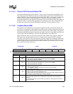
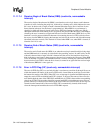
5LBM
Loopback mode.
0 – Normal serial port operation enabled.
1 – Output of transmit serial shifter is connected to input of receive serial shifter internally
and control of TXD3 and RXD3 pins is given to the PPC unit.
7..6 — Reserved.
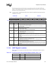
0h 8005 000C UTCR3 Read/Write
7 6 5 4 3 2 1 0
Reserved LBM TIE RIE BRK TXE
RXE
Reset
0 0 ? ? ? ? 0 0
(Sheet 2 of 2)
Bits Name Description