


130 SA-1110 Developer’s Manual
Memory and PC-Card Control Module
19 DWID2
DRAM data bus width for bank pair 2/3.
0 – 32 bits.
1 – 16 bits.
22..20 DRAC22..0
DRAM row address bit count for bank pair 2/3. This count includes one or two bits for
SDRAM bank selects.
000 – 9 row address bits. (Select this for support of 9x9 and 9x8 DRAMs.)
001 – 10 row address bits. (Select this for support of 10x10, 10x9, and 10x8 DRAMs.)
010 – 11 row address bits. (Select this for support of 11x11, 11x10, 11x9, and 11x8 DRAMs.)
011 – 12 row address bits. (Select this for support of 12x12, 12x11, 12x10, 12x9, and 12x8
DRAMs.)
100 – 13 row address bits. (Select this for support of 13x11, 13x10, 13x9, and 13x8
DRAMs.)
101 – 14 row address bits. (Select this for support of 14x10, 14x9, and 14x8 DRAMs.)
110 – 15 row address bits. (Select this for support of 15x11 (16-bit data bus only), 15x10,
15x9, and 15x8 DRAMs.)
111 – Reserved.
See Table 10-8 for more information.
23 CDB22
Clock divide by 2 for bank pair 2/3.
0 – CAS waveform rotate register (MDCAS20, 21, 22) rotated every CPU clock. Required
for SDRAM.
1 – CAS waveform rotate register rotated every memory clock.
(CPU clock divided by 2.)
SDRAM requires CDB22 = 0. However, the frequency of the SDRAM bank pair 2/3 clock
(SDCLK 2) can be set to either the memory clock frequency
(MDREFR:K2DB2 = 0) or half the memory clock frequency (MDREFR:K2DB2 = 1).
27..24 TRP23..0
RAS precharge for bank pair 2/3.
TRP is encoded with the minimum number of memory clocks (minus 1) of nRAS/nSDCS
deassertion between transfers.
For SDRAM running at the full memory clock frequency, TRP determines the minimum
delay (TRP+1 memory cycles) from the first memory clock rising edge following data latch
for autoprecharge read command (READAP) to the memory clock edge upon which
subsequent row commands (bank activate, mode register set, self-refresh, or CBR) are
latched. The minimum delay from latching of READAP command to latching of subsequent
row commands is TDL+TRP+2 memory cycles. The minimum delay from command and
data latching for autoprecharge write (WRITEAP) to latching of subsequent row commands
is TRP+TWR+1 memory cycles. TRP must be written to a value of at least 1 for SDRAM.
The unit size for TRP is always the internal memory cycle, even if SDRAM is run at half the
memory clock frequency (MDREFR:K2DB2 = 1). However, for SDRAM running at half
frequency, the unit size for TDL is two memory cycles and TRP is effectively increased by
one (because setup time for commands and write data is increased by one memory cycle).
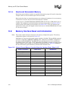
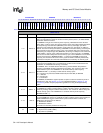
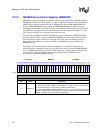
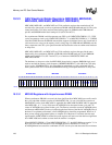
0h A000 0000 MDCNFG Read/Write
31 30 29 28 27 26 25 24 23 22 21 20 19 18 17 16 15 14 13 12 11 10 9 8 7 6 5 4 3 2 1 0
TWR21
TWR20
TDL21
TDL20
TRP23
TRP22
TRP21
TRP20
CDB22
DRAC22
DRAC21
DRAC20
DWID2
DTIM2
DE3
DE2
TWR01
TWR00
TDL01
TDL00
TRP03
TRP02
TRP01
TRP00
CDB20
DRAC02
DRAC01
DRAC00
DWID0
DTIM0
DE1
DE0
Reset ? ? ? ? ? ? ? ? ? ? ? ? ? ? 0 0 ? ? ? ? ? ? ? ? ? ? ? ? ? ? 0 0
(Sheet 3 of 4)
Bits Name Description