


142 SA-1110 Developer’s Manual
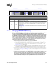
Memory and PC-Card Control Module
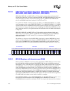
10.3.5 Expansion Memory (PC-Card) Configuration Register
(MECR)
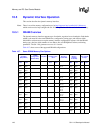
MECR is a read/write register that contains control bits for configuring the timing of the PC-Card
interface. This register is unaffected by reset; question marks indicate that the values are unknown
at hardware or sleep reset.
The programming of each of the six BS_xx fields allows the user to individually select the duration
of accesses to I/O, common memory, and attribute memory for each of two PC-Card card slots.
Each BS_xx field is identical and represents the number of memory clocks per tick of an internal
clock, referred to as BCLK. BCLK clocks the internal PC-Card state machine. See Figure 10-22
for a description of the PC-Card timing diagram.
When an access to a PC-Card address space is detected, the appropriate BS_xx field is selected
based on the memory map. Every (BS_xx + 1) memory clock cycles, a BCLK tick is generated to
advance the PC-Card state machine. All signals (except nPWAIT, which is asynchronous) on the
PC-Card bus are driven or sampled relative to this internal clock, although the clock itself is not
externally available. Table 10-5 shows the number of processor clocks per BCLK tick for each
BS_xx value. Table 10-6 shows the internal BCLK cycle times for each BS_xx setting given a
processor core frequency of 160MHz (6.25-ns cycle time).
Note: The BCLK speed for a given setting will change if the processor frequency changes.
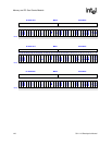
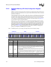
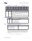
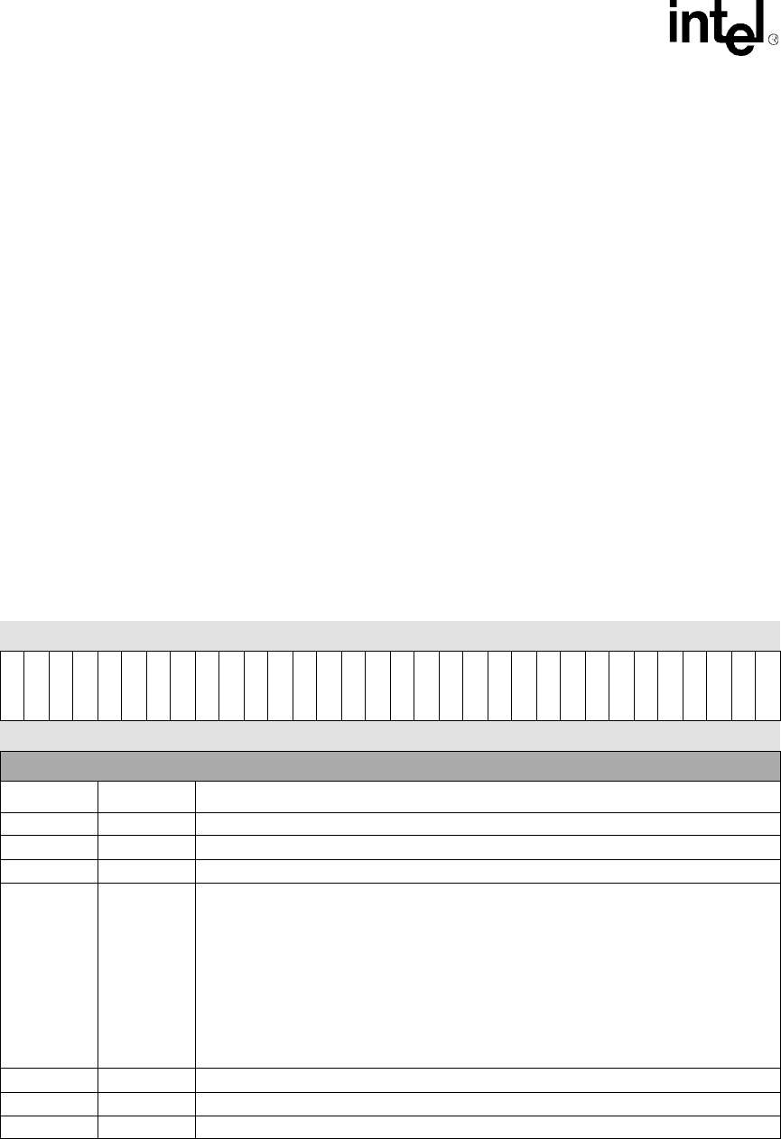
0h A000 0018 MECR Read/Write
31 30 29 28 27 26 25 24 23 22 21 20 19 18 17 16 15 14 13 12 11 10 9 8 7 6 5 4 3 2 1 0
FAST1
BSM1_4
BSM1_3
BSM1_2
BSM1_1
BSM1_0
BSA1_4
BSA1_3
BSA1_2
BSA1_1
BSA1_0
BSIO1_4
BSIO1_3
BSIO1_2
BSIO1_1
BSIO1_0
FAST0
BSM0_4
BSM0_3
BSM0_2
BSM0_1
BSM0_0
BSA0_4
BSA0_3
BSA0_2
BSA0_1
BSA0_0
BSIO0_4
BSIO0_3
BSIO0_2
BSIO0_1
BSIO0_0
Reset ? ? ? ? ? ? ? ? ? ? ? ? ? ? ? ? ? ? ? ? ? ? ? ? ? ? ? ? ? ? ? ?
(Sheet 1 of 2)
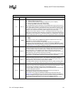
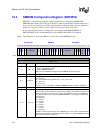
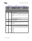
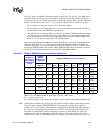
Bits Name Description
4..0 BSIO0 4..0 Memory clock count for accesses to PC-Card card slot 0, I/O space.
9..5 BSA0 4..0 Memory clock count for accesses to PC-Card card slot 0, attribute space.
14..10 BSM0 4..0 Memory clock count for accesses to PC-Card card slot 0, common memory space.
15 FAST0
Fast mode bit for access to slot 0 I/O, attribute, or memory.
If FAST0=1, the set-up time from address generated signals (A, nPREG, PSKTSEL and
nPCE) to initial assertion of the read or write strobe (nPWE, nPIOW, nPOE, or nPIOR) is
1*(BS_xx + 1) + 1 instead of the normal 3*(BS_xx + 1) + 1.
During I/O accesses, the nPCE set-up time is always reduced from these values by any
A-to-nIOIS16 delay.
The set-up time from address generated signals to the assertion of the read or write strobe
for the second half of a 16-bit access to 8-bit I/O is 2*(BS_xx + 1) instead of 1*(BS_xx + 1).
The duration of the read or write strobe remains 3*(BS_xx + 1), regardless of the value of
FAST0.
20..16 BSIO1 4..0 Memory clock count for accesses to PC-Card card slot 1, I/O space.
25..21 BSA1 4..0 Memory clock count for accesses to PC-Card card slot 1, attribute space.
30..26 BSM1 4..0 Memory clock count for accesses to PC-Card card slot 1, common memory space.