


SA-1110 Developer’s Manual 147
Memory and PC-Card Control Module
10.4.1 Changing SMROM RAS Latency
Whenever SMROM RAS latency is changed, a careful software sequence is required to coordinate
the SA-1110 with the SMROM devices. Otherwise, code fetches and/or data loads may be
corrupted by discrepancies between the contents of SMCNFG, MDCAS, and mode registers inside
the SMROM. The following sequence is appropriate for changing the RAS latency of bank pair 0/1
while it is serving instruction fetches (for example, during boot code following hardware or sleep
reset). A similar sequence is required for changing RAS latency of either bank pair when it is not
serving instruction fetches. The objective is to fetch and execute store instructions for changing
SMCNFG and MDCAS without any intervening SMROM reads.
1. Without changing RAS latency, enable burst reads from SMROM.
a. Write MDCAS00, MDCAS01, and MDCAS02 with present number of leading 1’s, but
filled through the 96th bit with the 2-bit repeating pattern of "0" followed by "1" (see
Section 10.3.3.2 for explanation).
b. Force a mode register set (MRS) command by writing SMCNFG with its present value.
The MRS configures the SMROMs’ internal mode registers for a burst length of eight.
2. If the instruction cache is not already enabled, enable it by setting bit 12 of the coprocessor 15
control register (see Chapter 6 and Chapter 5). This causes subsequent fetches to be performed
as 8-word bursts.
3. Align the store instruction which alters SMCNFG:RL0 to an 8-word address boundary. Locate
the store instructions that alter MDCAS00, MDCAS01, and MDCAS02 at the subsequent
three addresses. Aligning the four instructions to the start of a cache line ensures that they are
fetched together and executed prior to the next SMROM read. The store to SMCNFG will
cause another MRS command, which configures the desired RAS and CAS latencies.
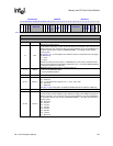
31 RL2
RAS latency for bank pair 2/3
It is the RAS-to-CAS delay (number of external SDCLK cycles between ACT command and
READ command). The unit size for RL2 is the external SDCLK cycle: when SMROM is run
at half the memory clock frequency (MDREFR:K0DB2 = 1), the delay is 2*RL2 internal
memory cycles.
See Section 10.4.1 for description of the software sequence required whenever changing
the RAS latency.
0-1clock
1 - 2 clocks
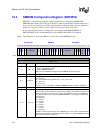
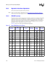
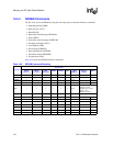
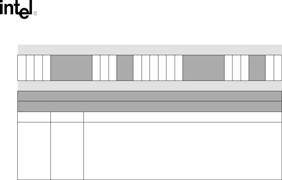
0h A000 0030 SMCNFG Read/Write
31 30 29 28 27 26 25 24 23 22 21 20 19 18 17 16 15 14 13 12 11 10 9 8 7 6 5 4 3 2 1 0
RL2
CL22
CL21
CL20
Reserved
RA22
RA21
RA20
Reserved
SM3
SM2
RL0
CL02
CL01
CL00
Reserved
RA02
RA01
RA00
Reserved
SM1
SM0
Reset ? ? ? ? ? ? ? ? ? ? ? ? ? ? 0 0 1 1 0 0 ? ? ? ? ? 1 0 0 ? ? 0 *
* Upon hardware or sleep reset, SM0 is set to the value of the SMROM_EN pin.
(Sheet 3 of 3)
Bits Name Description