


SA-1110 Developer’s Manual 121
Memory and PC-Card Control Module
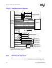
The SA-1110 external memory interface supports the following interfaces:
• Dynamic Memory Interface
The dynamic memory interface supports four 16-bit or 32-bit wide banks of asynchronous memory
(FPM or EDO) or synchronous DRAM. Each bank is allocated 128 Mbytes of the internal memory
map. However, the actual size of each bank is dependent on the particular DRAM configuration
used. The four banks are divided into two bank pairs: the 0/1 pair and the 2/3 pair. Both banks
within a pair (for example, bank 0 and bank 1) must be identical in size and configuration, but the
two pairs can be different (for example, the 0/1 pair can be 100 MHz SDRAM on a 32-bit data bus
while the 2/3 pair is 60 ns EDO DRAM on a 16-bit data bus).
There are 4 bank selects, nRAS/nSDCS[3:0], 4 byte selects, nCAS/DQM[3:0], 15 bits of
multiplexed row and column addresses, A[24:10], a write enable, nWE, and an output enable, nOE.
When SDRAM is used, some of the signals perform different functions and are complemented by
the nSDRAS, nSDCAS, SDCKE 1, and SDCLK[2:1] signals. The SA-1110 performs CAS before
RAS refresh (CBR) during normal operation and supports self-refreshing DRAM during
power-down sleep mode. Two SDRAM/SMROM auto-power-down mode bits (MDREFR:EAPD
for clock enables, MDREFR:KAPD for clocks) can be set so that each pin (including SDCKE 1
and SDCLK[2:1]) is automatically deasserted whenever none of the corresponding banks is being
accessed.
• Static Memory Interface / Static Memory or Variable Latency I/O Interface
The static memory interface and the static memory or variable latency I/O interface have six chip
selects (nCS[5:0]) and 26 bits of byte address (A[25:0]) for access of up to 64 Mbyte of memory in
each of six banks. Each chip select is individually programmable for selecting one of the supported
static memory types. Nonburst ROM or Flash memory are supported on each of nCS[5:0], burst
ROM or Flash memory (with nonburst writes) are supported on each of nCS[5:0], SRAM is
supported on each of nCS[2:0], SRAM-like variable latency I/O is supported on each of nCS[5:3],
and synchronous mask ROM (SMROM) is supported on each of nCS[3:0]. The variable latency
I/O interface differs from SRAM in that it allows the use of data ready input signal, RDY, to force
the insertion of wait states. SMROM is supported only on 32-bit wide data busses. For all other
(asynchronous) static memory types, each chip select can be individually configured to a 16-bit or
32-bit wide data bus. nOE is asserted on reads and nWE is asserted on writes. For SRAM and
variable latency I/O, nCAS/DQM[3:0] are byte selects for both reads and writes.
The SA-1110 supports systems with both SRAM and DRAM (synchronous or asynchronous) by
ensuring at least three CPU clock cycles of nCAS/DQM[3:0] deassertion between any permutation
of SRAM (or variable latency I/O) access and DRAM activity (access, CBR, or self-refresh).
However, the recovery time between SRAM accesses must be set to satisfy the minimum
nCAS/DQM[3:0] deassertion time for any asynchronous DRAM present in the system.
When the SA-1110 comes out of reset, it begins fetching and executing instructions at address
0x00, which corresponds to memory selected by nCS0. This is where boot ROM is expected to be.
The SMROM_EN pin determines if the boot ROM is asynchronous or synchronous.
In addition to nCS[3:0], the static memory interface for SMROM uses write enable (nWE), output
enable (nOE), two of the SDRAM control signals (nSDRAS and nSDCAS), plus a clock enable
(SDCKE 0) and clock (SDCLK 0). The nWE pin is asserted for SMROM only when writing its
mode register. SMROM is supported only on 32-bit wide data busses. Two SDRAM/SMROM
auto-power-down mode bits (MDREFR:EAPD for clock enables, MDREFR:KAPD for clocks) can
be set so that each pin (including SDCKE 0 and SDCLK 0) is automatically deasserted whenever
none of the corresponding banks are being accessed.
• PC-Card Interface