


SA-1110 Developer’s Manual 387
Peripheral Control Module
11.13.5 PPC Pin Assignment Register
The UART in serial port 1 and the SSP in serial port 4 can be reassigned to GPIO pins using the
PPC pin assignment register (PPAR). The PPAR contains two bits that control the reassignment of
each serial engine to an individual set of GPIO pins.
11.13.5.1 UART Pin Reassignment (UPR)
The UART pin reassignment (UPR) bit selects whether the serial port 1 UART is assigned to GPIO
pins 14 and 15. When UPR=0, serial port 1 uses the TXD1 and RXD1 pins; the GPCLK/UART
select (SUS) bit selects which protocol to enable. When UPR=1, SUS is ignored, serial port 1
defaults to the GPCLK operation mode. This configures the UART to use GPIO<14> for transmit
and GPIO<15> for receive.
11.13.5.2 SSP Pin Reassignment (SPR)
The SSP pin reassignment (SPR) bit is used to select whether serial port 4’s SSP is assigned to GPIO pins
10 through 13. When SPR=0, serial port 4 uses its TXD4, RXD4, SCLK, and SFRM pins; the MCP
enable (MCE) and SSP enable (SSE) bits are used to select which protocol is enabled (MCE has
precedence over SSE). When SPR=1, MCE and SSE must both be set; serial port 4 defaults to MCP
operation using the TXD4, RXD4, SCLK, and SFRM pins, and the SSP is configured to use GPIO 10 for
transmit, GPIO 11 for receive, GPIO 12 for serial clock, and GPIO 13 for serial frame. Note that the user
must set bits 10 through 13 in the GPIO alternate function register (GAFR) as well as set bits 10, 12, and
13 and clear bit 11 in the GPIO pin direction register (GPDR). See the Section 9.1, “General-Purpose
I/O” on page 9-73.
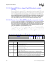
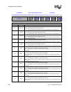
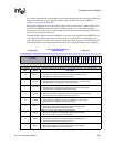
19 RXD4
Serial port 4: MCP/SSP receive pin state.
Read – Current state of serial port 4 receive pin returned.
Write – If serial port 4 receive disabled and pin configured as an output, drive value to
receive pin.
20 SCLK
Serial port 4: MCP/SSP serial clock pin state.
Read – Current state of serial port 4 serial clock pin returned.
Write – If serial port 4 disabled and pin configured as an output, drive value to serial clock
pin.
21 SFRM
Serial port 4: MCP/SSP serial frame pin state.
Read – Current state of serial port 4 serial frame pin returned.
Write – If serial port 4 disabled and pin configured as an output, drive value to serial frame
pin.
31..22 — Reserved.
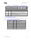
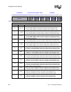
0h 9006 0004 PPC Pin State Register: PPSR Read/Write
31 30 29 28 27 26 25 24 23 22 21 20 19 18 17 16 15 14 13 12 11 10 9 8 7 6 5 4 3 2 1 0
Reserved
SFRM
SCLK
RXD4
TXD4
RXD3
TXD3
RXD2
TXD2
RXD1
TXD1
L_BIAS
L_FCLK
L_LCLK
L_PCLK
LDD 7
LDD 6
LDD 5
LDD 4
LDD 3
LDD 2
LDD 1
LDD 0
1 1 1 1 1 1 1 1 1 1 ? ? ? ? ? ? ? ? ? ? ? ? ? ? ? ? ? ? ? ? ? ?
(Sheet 2 of 2)
Bits Name Description