


SA-1110 Developer’s Manual 173
Memory and PC-Card Control Module
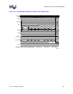
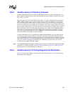
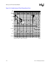
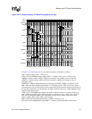
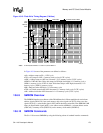
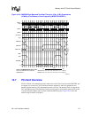
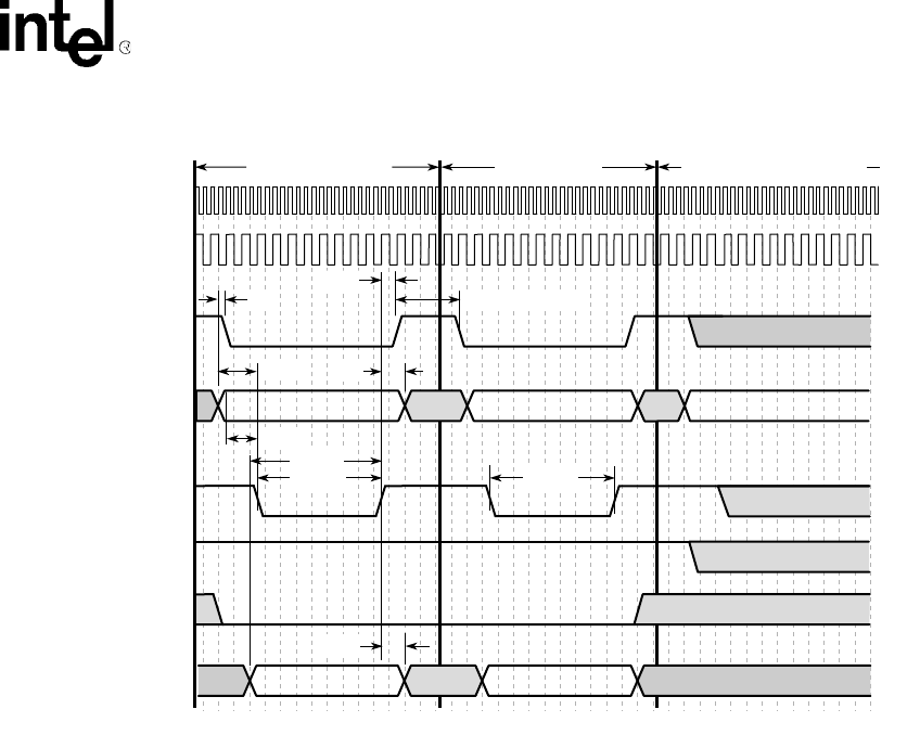
Figure 10-16. Flash Write Timing Diagram (2 Writes)
Note: If RT=00 then RDN+1. If RT=1x, then RDF+1
In Figure 10-16 some of the parameters are defined as follows:
tAS = Address setup to nCS = 1 CPU cycle
tCES = nCS setup to nWE = 2 memory clock cycles (4 CPU cycles)
tASW = Address setup to nWE low (asserted) = 2-1/2 memory cycles (5 CPU cycles)
tDSWH = If RT=00, then: Write data setup to nWE high (deasserted) = 1/2 memory cycle +
(RDN+1) memory cycles. If RT=1x, then: Write data setup to nWE high (deasserted) = 1/2
memory cycle + (RDF+1) memory cycles.
tDH = Data hold after nWE high = 1+1/2 memory cycle
tCEH = nCS held asserted after nWE deasserted = 1 memory clock cycle (2 CPU cycles)
tAH = Address hold after nWE deasserted = 1+1/2 memory cycle (3 CPU cycles)
10.6.9 SMROM Overview
The SMROM interface uses thirteen of the DRAM interface’s fifteen multiplexed row/column
address signals (DRA12-0), four static memory chip select signals (nCS[3:0]), thirty-two data
signals (D[31:0]), a write enable signal (nWE) which should be connected to the SMROM’s MR
input, an output enable signal (nOE), a row address strobe (nSDRAS), a column address strobe
(nSDCAS), a memory clock (SDCLK 0), and a memory clock enable (SDCKE 0).
10.6.10 SMROM Commands
The SA-1110 accesses SMROM by using the following subset of standard interface commands:
A6656-02
CPU
Clock
Memory
Clock
A(25:0)
nCS0
Write Command
nOE
RD/nWR
D(31:0)
nWE
DataCMD
Write Data Possible Read or Write
t
AS
t
ASW
t
CES
t
DH
RDN+1 RDN+1
max (2*RRR,1)
t
CEH
t
AH
A0 A1
t
DSWH